
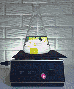
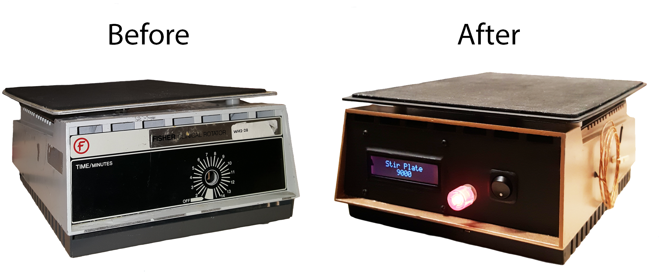
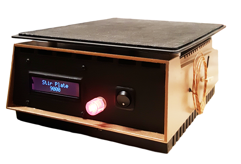
Recently I came across an old chemistry lab stir plate made by Fisher. I thought it would be a fun weekend project to restore it and add some functionality. Here’s a before and after shot of the project.
Keep scrolling down if you’re interested in more detail!
In addition to restoring the paint, the features that I added are as follows:
- Adjustable speed (5 to 150 RPM)
- Adjustable direction
- User interface (LCD + Rotary Encoder + Piezo Buzzer)
- K-Type Thermocouple for temperature readings (-200 to 500°C)
- Shake mode
- Stir mode
The microcontroller used in this project is a 16-bit PIC24FJ64GA002.
The C code written for this project can be seen here.
Case
The stripping process:
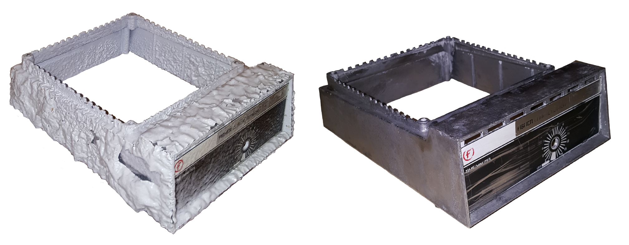
After the case was clear of old paint and debris, I dremeled out the face plate to make room for the LCD and a switch. I used the hole that was already there for the rotary encoder. Additionally, I cut a port out in the back so that I could add a fused switch for the AC connection.
Finally, I rinsed the case in mineral spirits, applied a primer coat, and then the paint.
Motor
The original motor found in the stir plate is similar to those used to rotate a plate of food in a home microwave. It is an Autotrol permanent magnet synchronous AC gear motor.
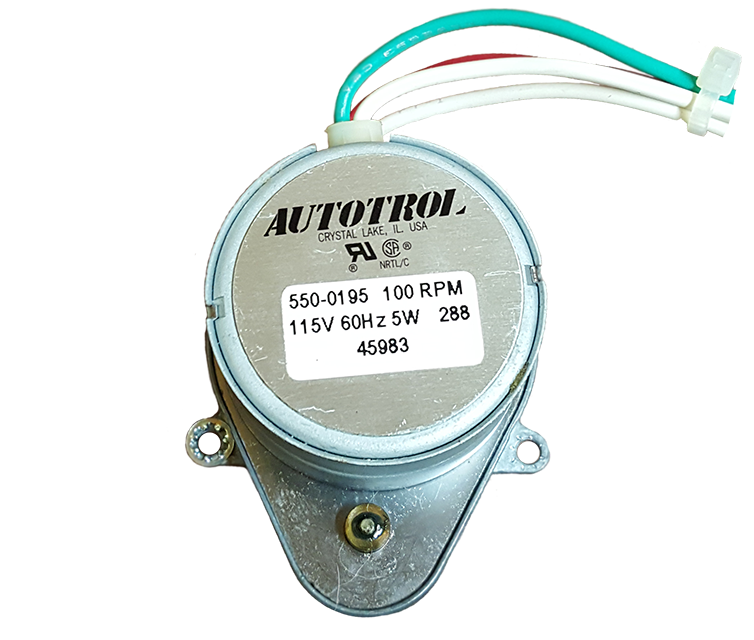
These motors can be controlled only by varying the AC’s frequency or by changing their gear ratio, neither of which are cheap or ideal for this application.
The motor that will be used instead is a uni-polar stepper motor.

I chose to use a stepper motor given that stepper motors are inexpensive and do not require additional feedback components to achieve precise control. This particular stepper motor can provide up to 88.3 N·cm of holding torque which should be more than enough for this application.
To control the stepper motor, an A3967 Microstepping Stepper Motor Driver will be used. These guys can be easily implemented thanks to Brian Schmalz’s Easy Driver.
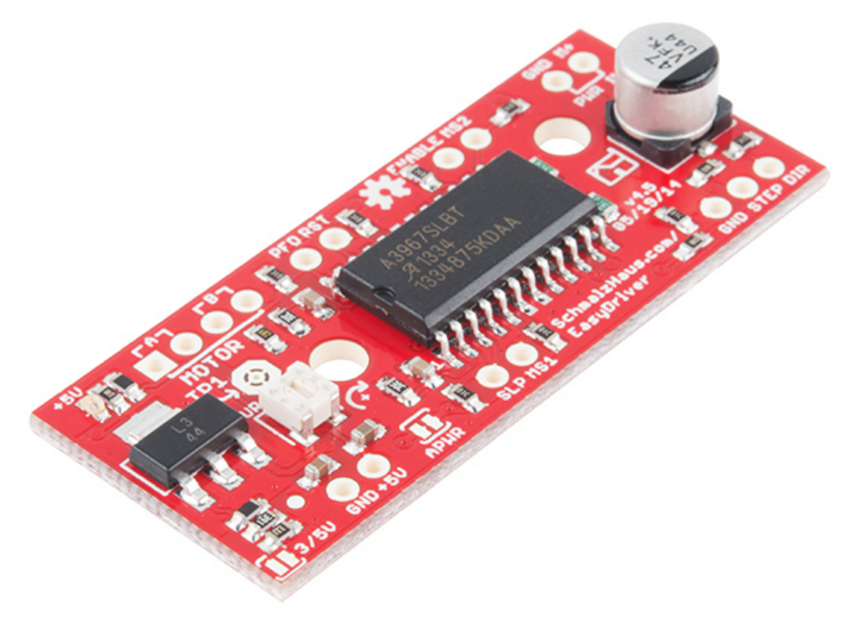
The Easy Driver is supplied with 6-30 volts and can be configured to deliver full steps or micro steps. It is designed to drive bi-polar stepper motors or uni-polar steppers wired as bi-polar. It can supply up to 700 mA to each phase.
A single step is achieved by sending a 3.3 V pulse to the Easy Driver. This particular stepper motor will complete one revolution every 200 steps, so a pulse frequency of 200 Hz correlates to a rotation of 1 revolution per second.
I found that the motor operated much more smoothly when the Easy Driver was configured to operate in micro step mode. Rather than taking a full step each pulse, the stepper motor will take an 8th of a step, or one revolution for every 1600 pulses. This scheme is ideal for microcontrollers that can deliver a pulse width modulation (PWM) signal.
Two factors influence the PWM signal that is generated by the microcontroller: the period (how often a pulse is generated) and the duty cycle (the ratio of high to low within the period).
The period can be controlled using a hardware timer configured as an interrupt source. The period is set by assigning a value to the “period register”.
The duty cycle can be controlled by comparing the timer’s value with a threshold value known as the “output compare” value. If the counter’s value is less than the OC value, the designated pin will be driven high, if the counter’s value exceeds the OC value, the pin will be driven low.
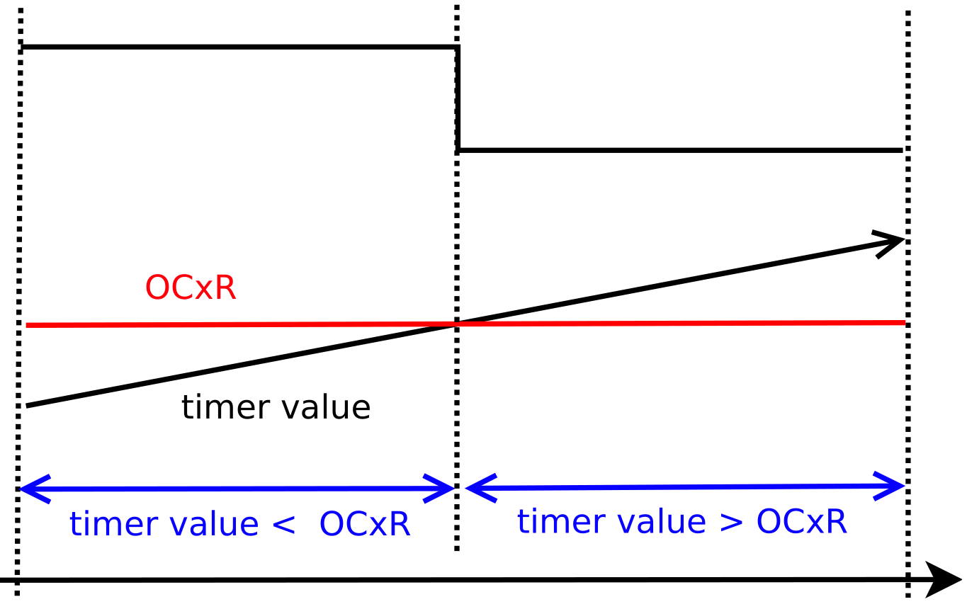
By changing the values stored in the period register and the output compare register, the PWM’s frequency and duty cycle can be set. This is what will allow the user to precisely adjust the RPM of the stir plate. The duty cycle will be configured to always remain at 50%.
Power
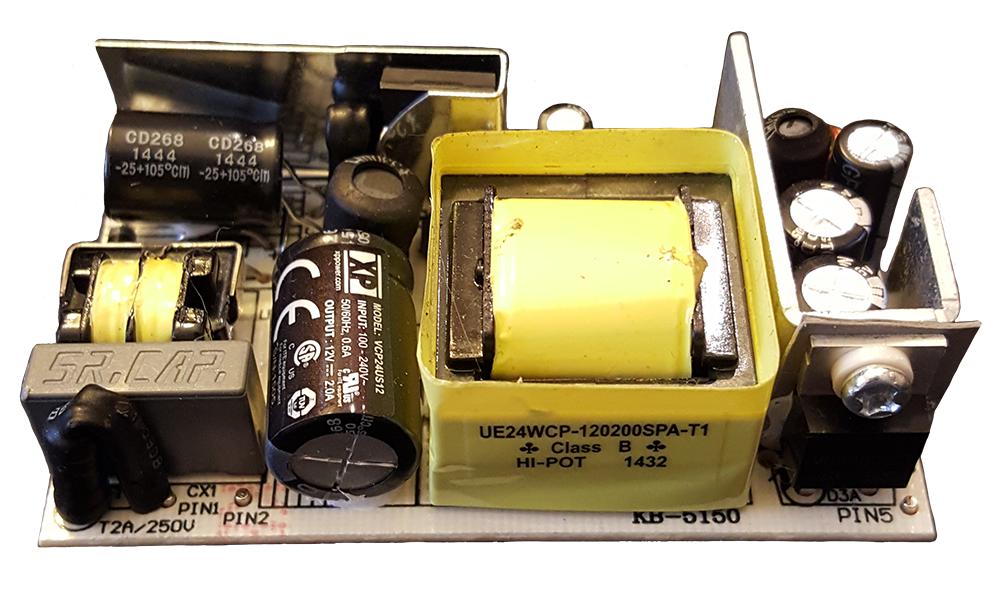
Because stepper motors require direct current, an AC/DC converter will be required. To achieve the necessary DC voltage rails for this project, I will have to convert the 120 VRMS AC coming from the wall to 12 VDC and 3.3 VDC. The 12 VDC will come from a transformer/full-wave bridge rectifier, while the 3.3 VDC will come from a linear LDO regulator that will cascade the rectifier.
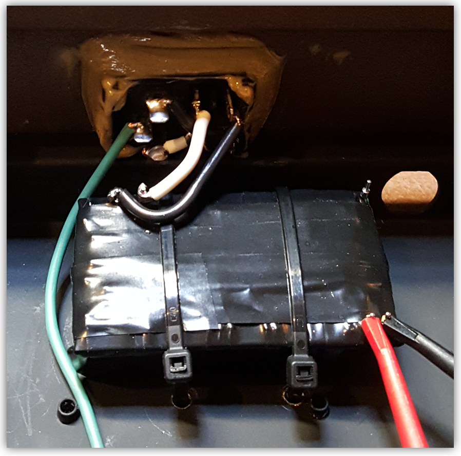
To preserve the AC/DC converter and make it safer, I sealed it in many wrappings of electrical tape. I attached the grounding wire to the case and sanded down all of the contacts to deter current from passing through a human to earth ground in the event that the AC shorts to the case and someone were to touch it.
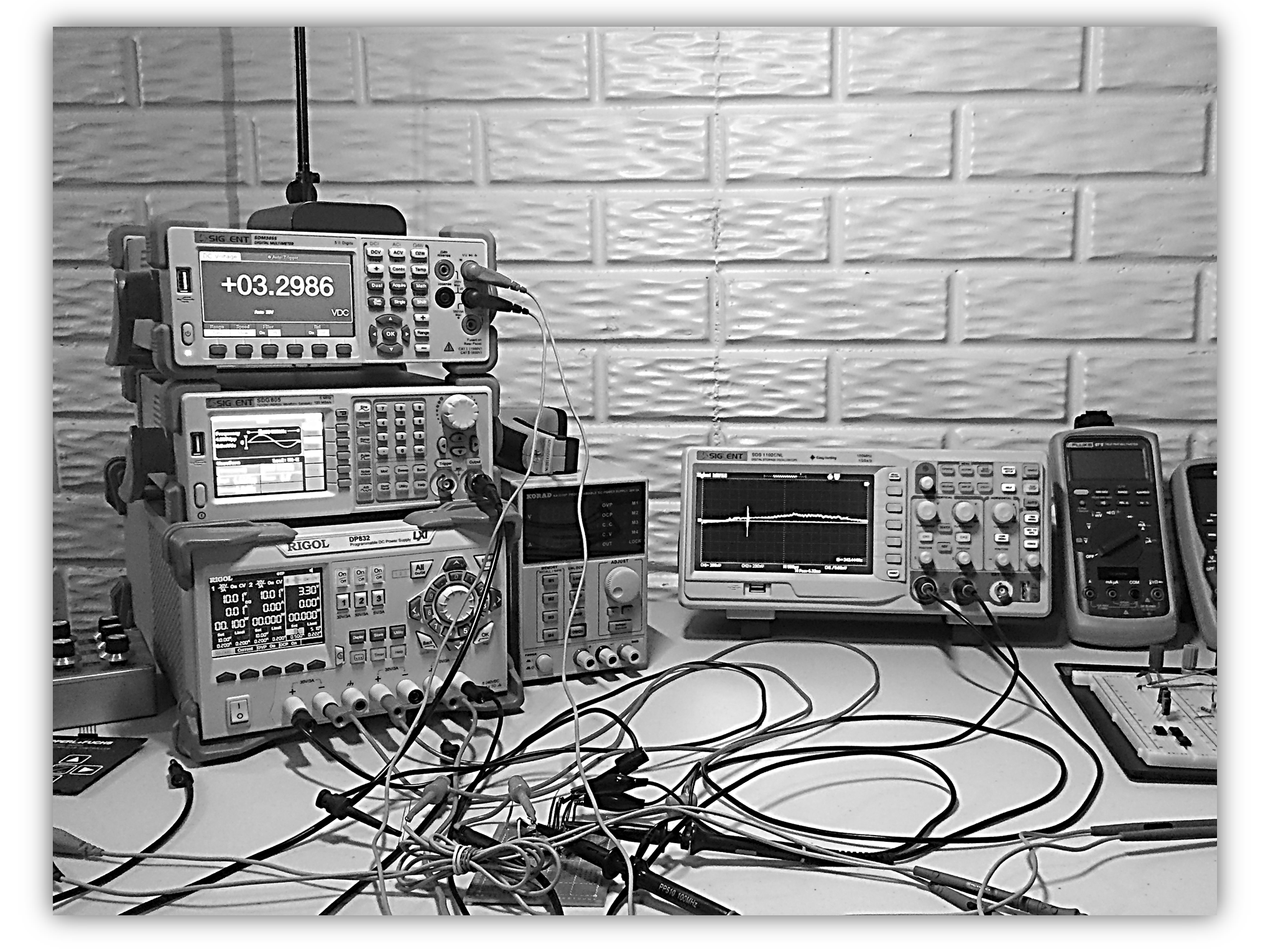
Now to verify the voltage rails…
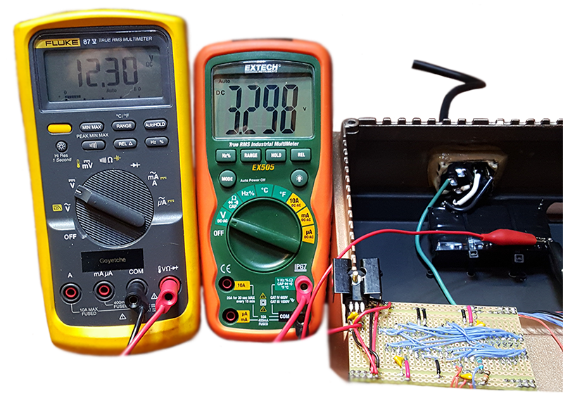
Great! 12.3 V @ 2 A for the stepper motor and 3.3 V @ 500 mA for the logic. The 3.3 V LDO is heat-sinked due to the fact that there is a 9 V voltage drop across it. To further verify that these PSUs are properly installed, I like to be sure there are no thermal issues under load.
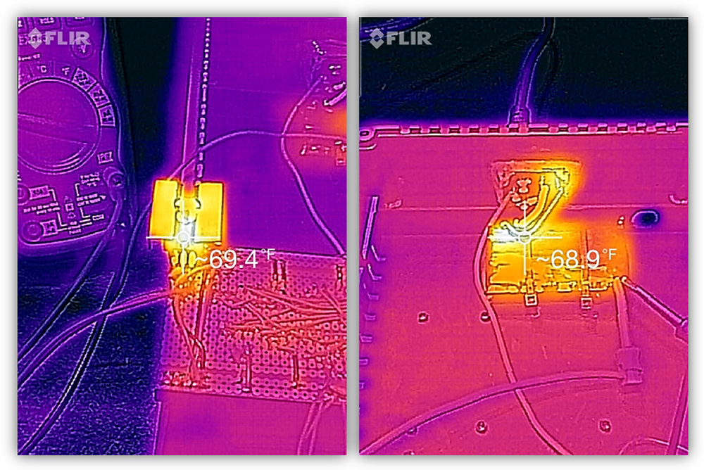
Looks good.
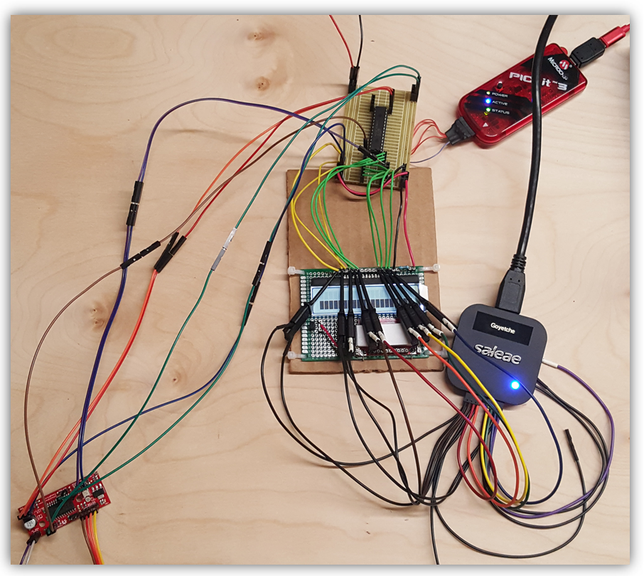
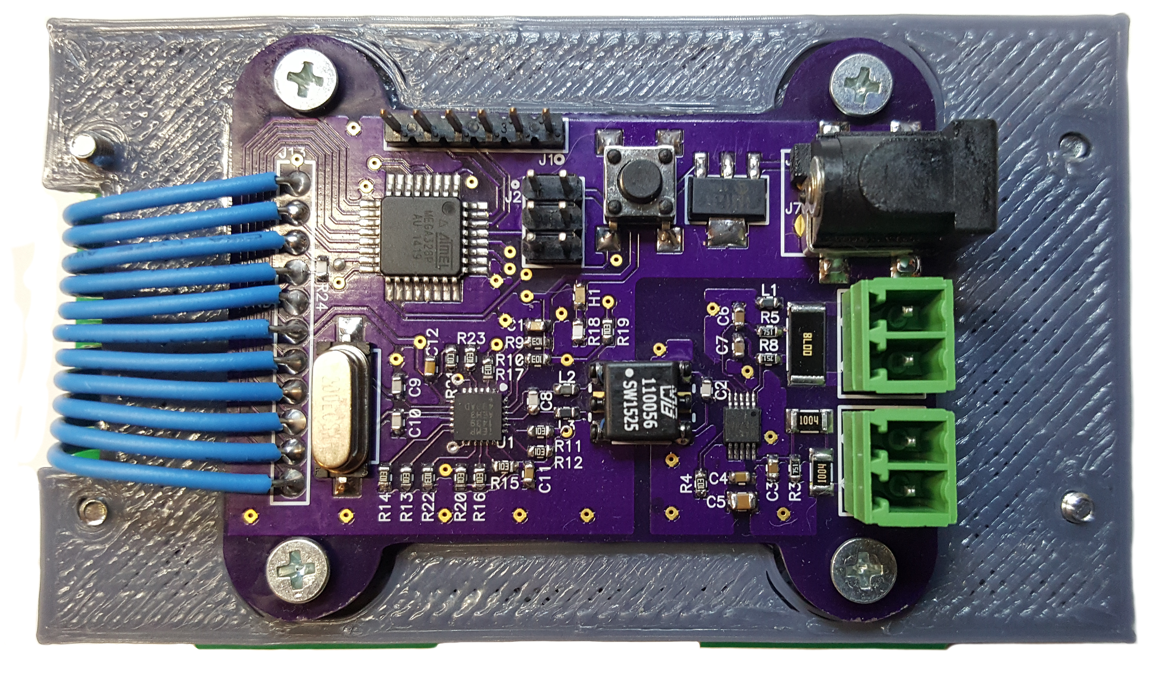
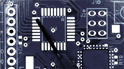
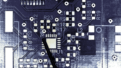
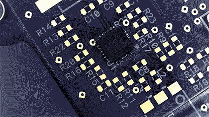
Control Board
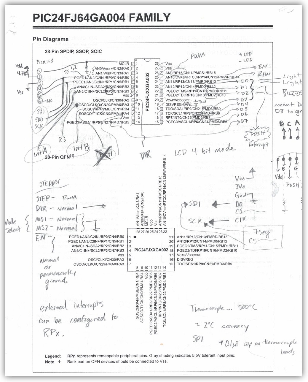
When implementing a controller into a project, I like to start by making a list of the I/O requirements (digital, analog, PWM, communication buses, etc…) and then comparing it to the controller’s datasheet to see if it meets the requirements of the project. In this case, I am just scratching out ideas on the PIC’s pin diagram.
Looks like this will do… now to solder up some proto-board with the basic essentials for the controller. This will be the initial platform for development. To make things easier on myself, I added some female headers and grouped them in order by their function. I then labeled the picture to print out as a reference for wiring.
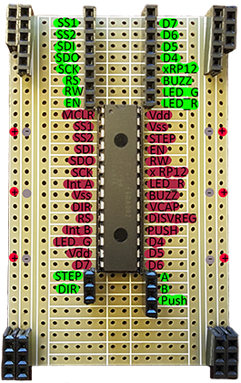
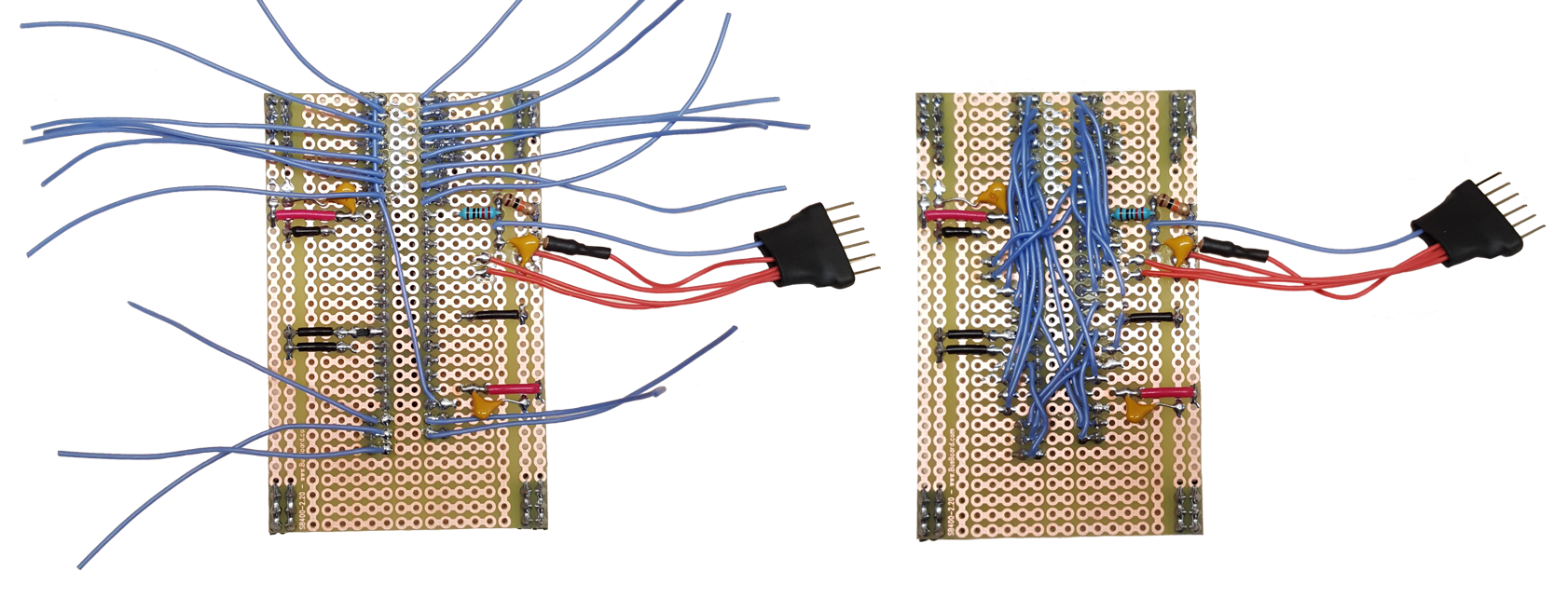
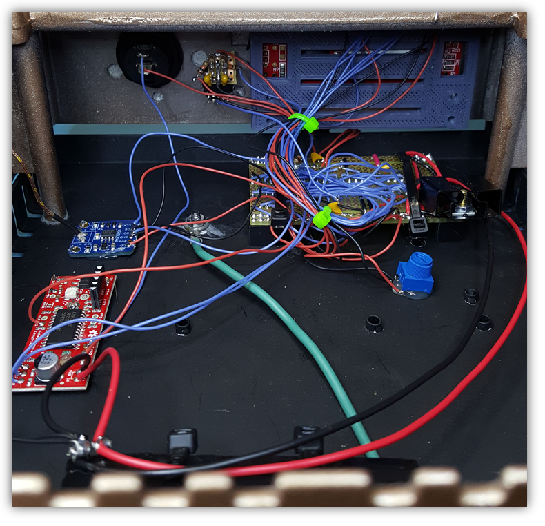
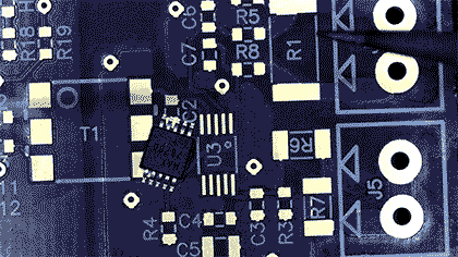
The proto-board is all wired and ready to begin coding with.
Thermocouple
To give the stir plate the ability to measure temperature, I will be adding a K-Type thermocouple with a MAX31855 thermocouple amplifier. This is similar to the thermocouple feature found on some multimeters.
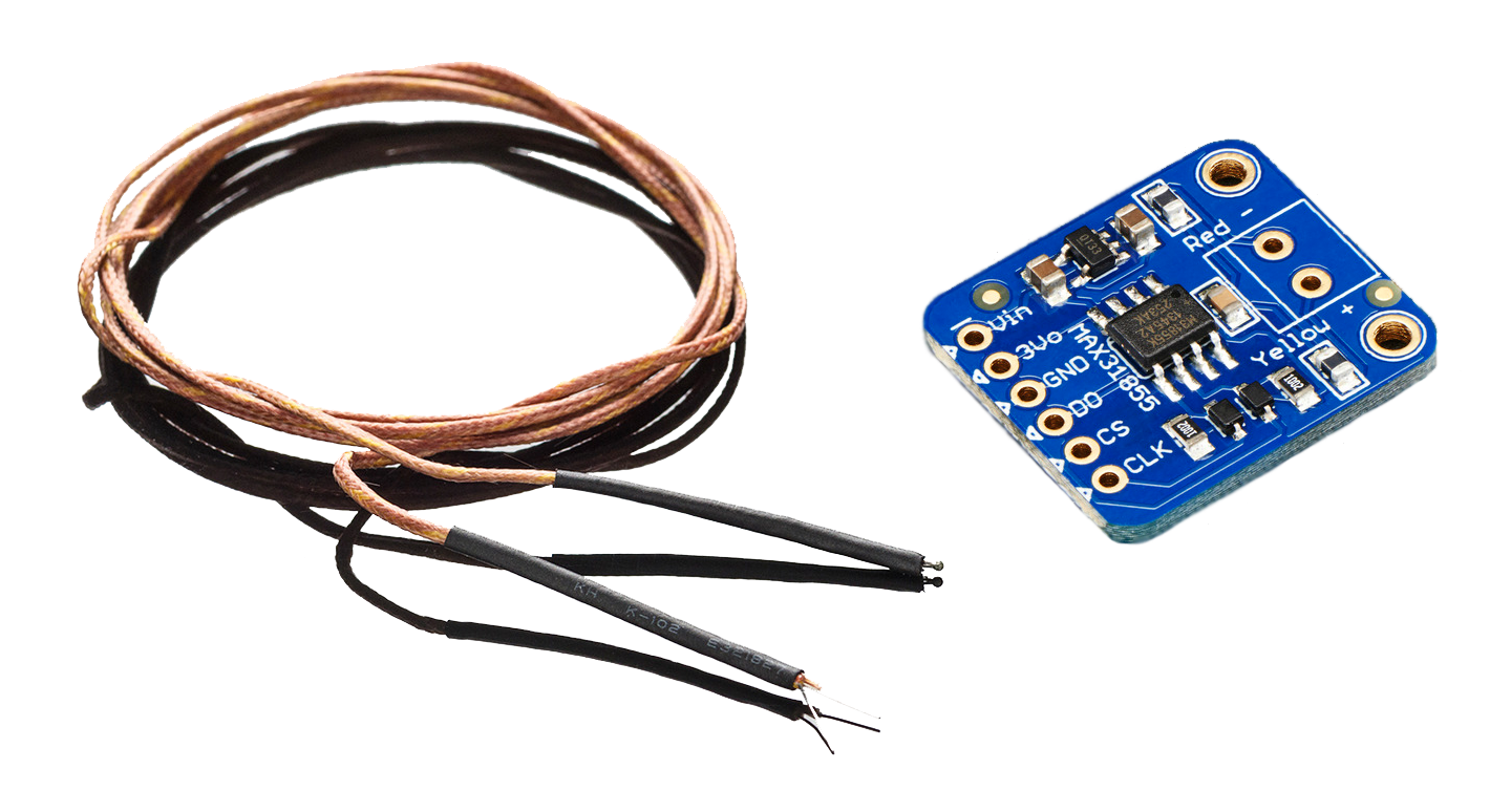
The thermocouple is made up of two dissimilar metals that are joined at two ends. In the case of this K-Type thermocouple, the alloys are Chromel and Alumel. This arrangement will produce a measurable voltage when there is a difference in temperature between its hot junction (measurement) and cold junction (reference). Because this voltage differential is small, a thermocouple amplifier will be used.
The MAX31855 will take in the analog voltage from the thermocouple, amplify it, digitize it, and finally encode it. This information is then available via a SPI bus, so the only work I need to do is to write a driver that will grab these bits and decode them for the display.
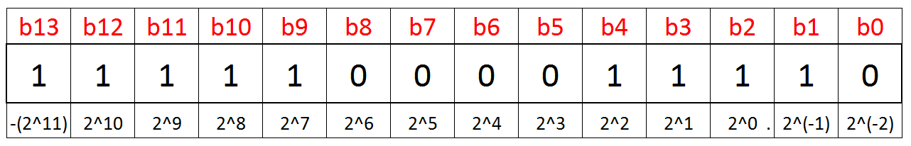
The protocol is simple. Each time the slave select is pulled low, the temperature data is refreshed. There are 32 bits of information, however, only the 14 most significant bits contain the temperature data, the rest can be dismissed. The MSB is the sign bit, the next 11 bits contain the whole number, and the last 2 bits contain the fractional portion (allowing for increments of 0.25 °C).
For example, if the temperature were -121.5 °C, the data frame of the 14 most significant bits would look like this:
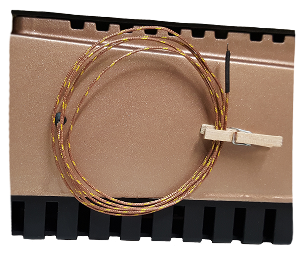
For storage, I added a tiny clothes pin to keep the thermocouple out of the way when it’s not being used.
User Interface
Display
The display that will be used in the user interface is a Hitachi HD44780 LCD. I am going to implement this in 4-bit mode, reducing the data pin requirements from 8 to 4 (this would have been a nightmare without a logic analyzer).
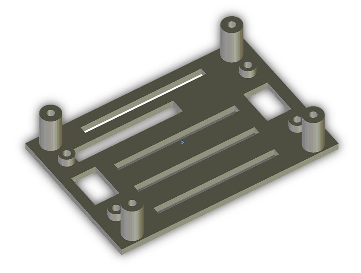
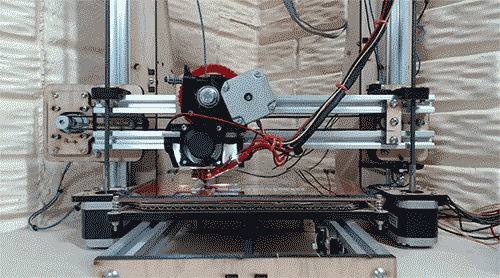
Now to come up with some kind of mounting bracket for the LCD. Here is the 3D model I generated in Blender and then printed on a Prusa i3.
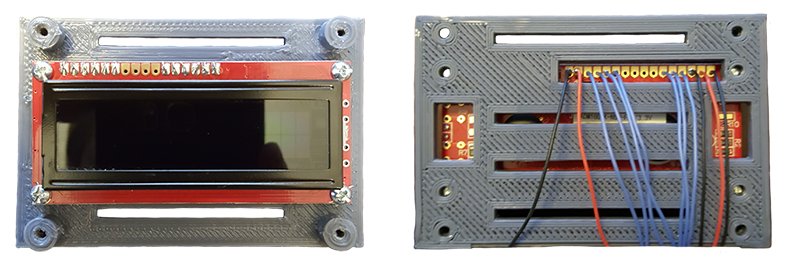
LCD and bracket assembled and wired:
User interface fully assembled and painted:
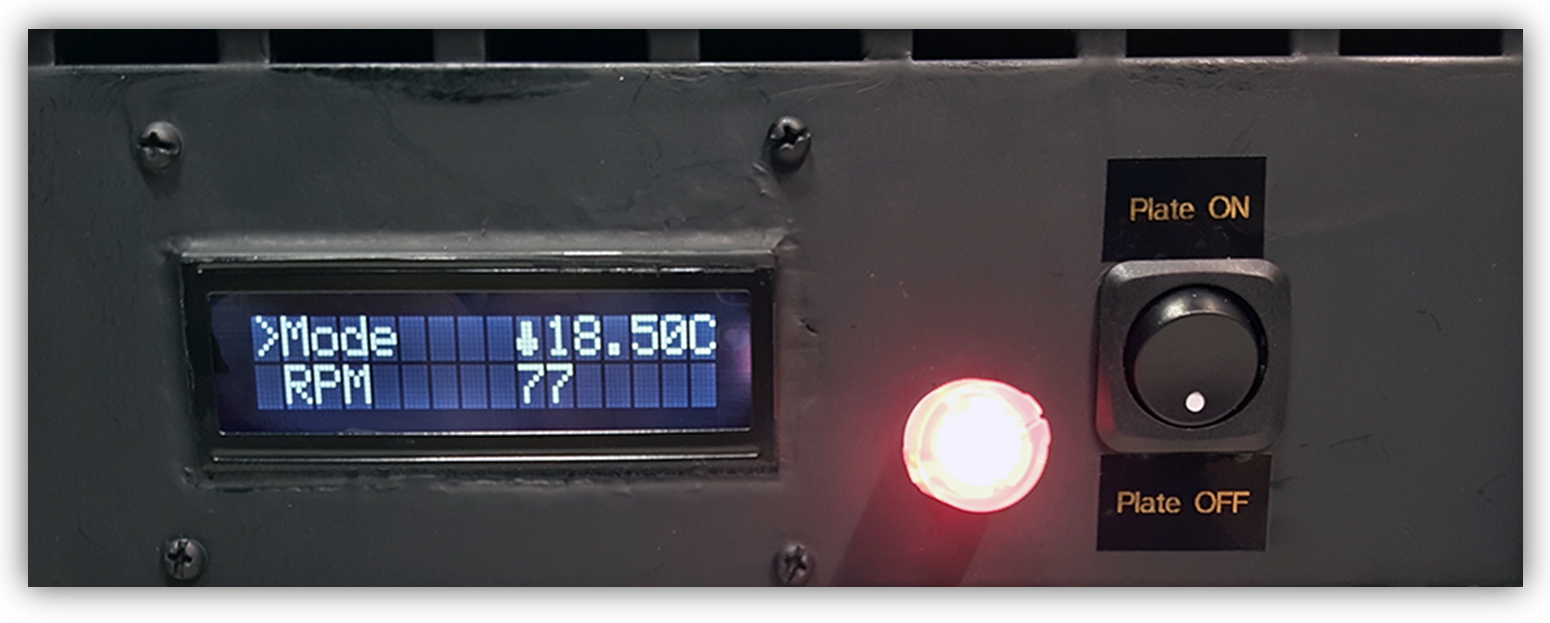
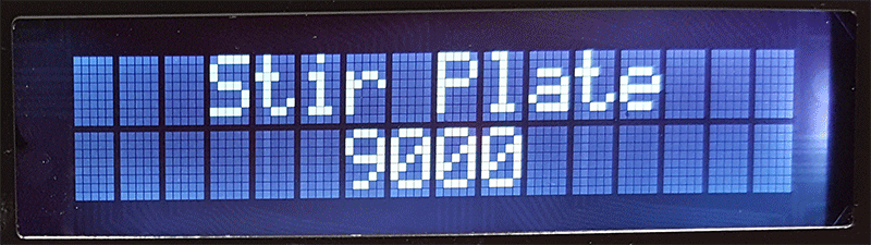
Here are some of the menus that can be navigated to with the rotary encoder. The rotary encoder is interrupt driven, so navigation is seamless even if the microcontroller is busy with another process.
Rotary Encoder
A rotary encoder is essentially a device that consists of two or three switches. There are two switches that are either normally open or normally closed that will briefly change state each time the knob is rotated. The direction of the turn can be deduced by detecting which switch changed state first. The third switch allows the knob itself to act as a momentary push button. This single device can allow a user to scroll through and select different menu options.
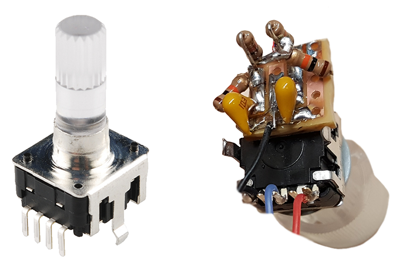
Because mechanical switching is occurring as the rotary encoder is operated, debouncing each switch with passive low-pass filters will improve its overall function.
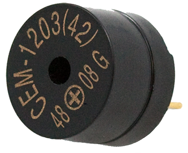
Audible Feedback Piezo Buzzer
Making an intuitive user interface is a challenge for any designer. It’s easy to navigate through something you designed, but the trick is to always stay in the mindset as if you were looking at it for the first time. Having haptic or audible feedback is a good way to let the user know that their input was received. Although the rotary encoder has distinguishable clicks, a piezo buzzer will generate an audible tone each time an input was successfully received.
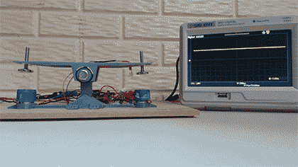
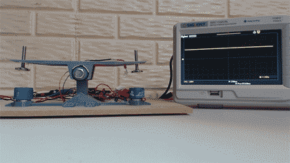
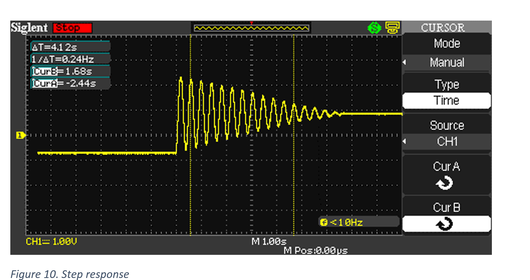
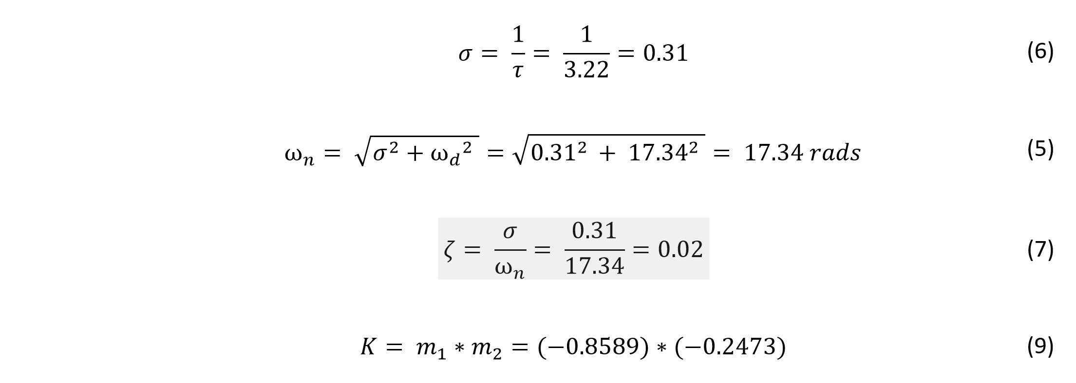
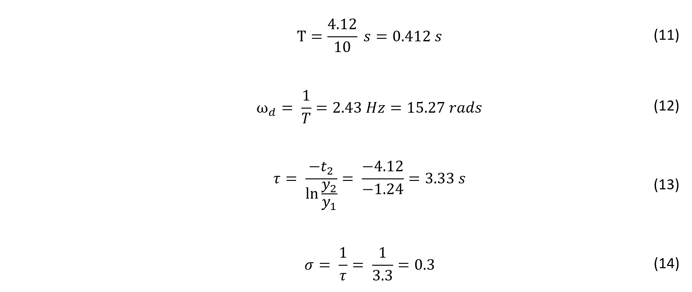
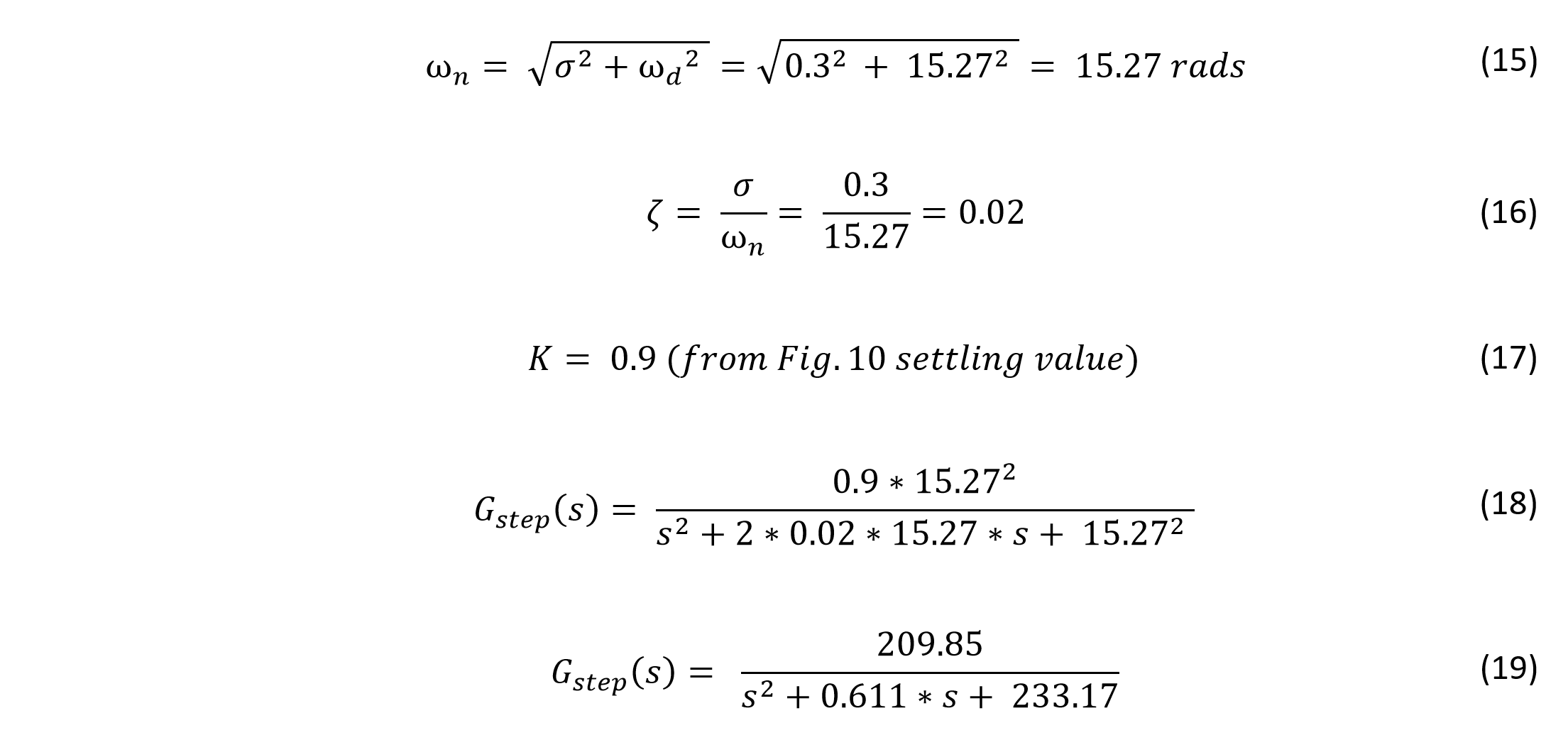
Results
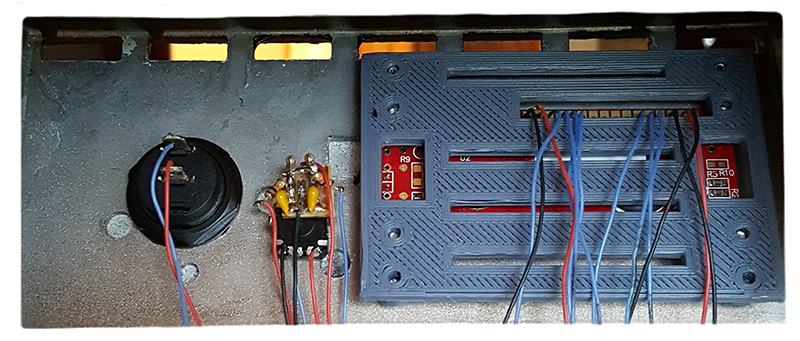
Final wiring:
Finished project:


