Ferrite Beads
noteWhat a ferrite bead actually is, why its datasheet number describes almost nothing about how it behaves in a circuit, how it resonates with the capacitance around it, why it does not belong in series with a digital signal or in a ground return, the narrow case where it is the right part, and what to do instead.
Scope: chip ferrite beads as used on power rails, signal lines, and ground connections in mixed-signal and digital boards. The note covers the part's real electrical behavior, the failure modes that follow from treating it as a generic noise filter, and the alternatives. Common-mode chokes for cables and power-line filter inductors are different parts and are mentioned only for contrast.
Common errors
- Treating "600 Ω at 100 MHz" as the part's impedance. It is one point on a curve. Below about 30 MHz the same part is a few ohms of nearly lossless inductance, and the inductance is what the circuit sees.
- Putting a bead in front of a capacitor without checking the resonance. Bead inductance and downstream capacitance form a second-order filter with a Q set by the bead's small DC resistance. The result peaks by 10 to 20 dB at a frequency that is often near the switching frequency of the regulator feeding it.
- Using the datasheet impedance at the operating current. Impedance collapses with DC bias. A small bead at half its rated current has lost most of its impedance; the rating is a heating limit.
- Putting a bead in series with a digital signal. It slows the edge, rings with the trace capacitance, and produces overshoot and threshold recrossings. A signal that needed slowing needs a resistor, and a signal that radiates needs a return path.
- Connecting two ground regions through a bead. Every return current that crosses the split flows through it, and the voltage across it appears as a shift between the two references.
- Adding a bead because the reference design has one. The reference design had a specific noise source, a specific capacitor, and a specific measurement behind that bead, or it did not and the bead is folklore. Neither transfers.
- Solving a layout problem with a component. Noise on a rail that is caused by a shared return path, a decoupling capacitor placed far from the pin, or a plane split is not filtered away. It is fixed by moving the copper.
What a ferrite bead is
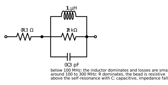 Figure 1. Equivalent circuit of a chip ferrite bead. A small DC resistance in series with a parallel combination of inductance, a loss resistance, and the winding and termination capacitance.
A chip bead is a short conductor through a block of lossy ferrite. The ferrite's permeability gives the conductor inductance, and the ferrite's loss, which rises with frequency, gives it a resistive component. The equivalent circuit is a DC resistance in series with a parallel inductance, loss resistance, and stray capacitance. All four elements change with frequency, temperature, and DC current, and the datasheet specifies one of them at one frequency.
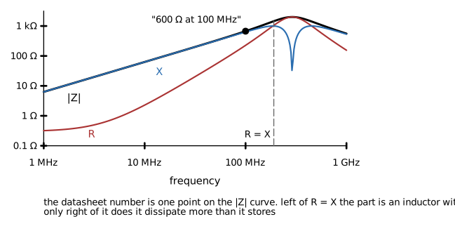 Figure 2. Impedance, resistance, and reactance versus frequency for a typical "600 Ω" bead. The datasheet figure is one point. Left of the R = X crossover the part is an inductor.
The impedance curve has three regions.
- Inductive, from DC to a few tens of megahertz. Impedance rises at 20 dB per decade, the phase is near 90°, and the loss is small. Energy put into the part is stored and returned, which is the property that makes it resonate with whatever capacitance it faces.
- Resistive, around the frequency where the loss resistance equals the reactance, typically 50 MHz to a few hundred megahertz. This is the region the part is sold for. Energy at these frequencies is dissipated as heat in the ferrite rather than reflected or stored.
- Capacitive, above the self-resonance with the stray capacitance. Impedance falls, and the part stops being a filter for anything above a few hundred megahertz to a gigahertz.
The datasheet gives the impedance magnitude at 100 MHz, the DC resistance, the rated current, and sometimes a curve of , , and against frequency at zero current. It does not give the inductance, which is what determines the behavior below the crossover, and it rarely gives the impedance at the rated current.
For the part in Figure 2, 6 Ω at 1 MHz gives about 1 µH. That number, not 600 Ω, is what the circuit sees at every frequency a switching regulator, an ADC clock, or an audio signal occupies.
Why the bead is poorly characterized
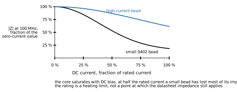 Figure 3. Impedance at 100 MHz against DC bias current for a small and a large bead. The core saturates well below the rated current.
DC bias. The ferrite saturates. A 0402 bead rated at 500 mA has typically lost half its impedance by 150 mA and three quarters by 400 mA. The rated current is the current at which the part's temperature rise reaches the datasheet limit; it says nothing about impedance. Manufacturers that publish bias curves show them at 100 MHz; the inductance in the region that matters falls with the same core, so the resonance frequency moves with load current.
Tolerance. The impedance at 100 MHz is typically ±25 %. The inductance, being unspecified, has no tolerance at all, and the crossover frequency between vendors' parts with the same nominal impedance and footprint can differ by a factor of two. A second-source substitution changes the filter.
Temperature. Ferrite permeability and loss both change with temperature. Impedance can fall by 20 to 40 % between 25 °C and 85 °C, and by more at the Curie temperature of the material, which for some beads is near 125 °C.
Frequency. Nothing about the part is constant across the band. A filter built from it has a corner and a Q that depend on where the noise is, and the noise in a mixed-signal board occupies the entire range from the regulator's switching frequency to the clock harmonics.
A resistor is characterized to 1 % across its range. An inductor is characterized to 10 or 20 % with a stated saturation current and self-resonance. A bead is characterized at one frequency and one current, and its behavior everywhere else is inferred. That is the sense in which it is a poorly characterized inductor: it is an inductor whose inductance is not on the datasheet.
Resonance with the capacitance around it
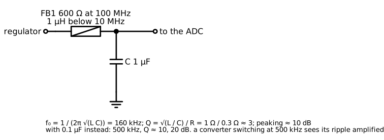 Figure 4. Bead on a supply rail feeding a bypass capacitor. Below the bead's resistive region this is an LC filter with a resonance and a Q set by the DC resistance.
The usual placement is in series with a supply rail, followed by the load's bypass capacitor. Below the crossover the bead is an inductor, and an inductor followed by a capacitor is a second-order low-pass with
The damping resistance is the bead's DC resistance plus the source impedance of whatever feeds it plus the capacitor's ESR, all of which are small. With a 1 µH bead and 1 µF of ceramic, is 160 kHz, is 1 Ω, and with 0.3 Ω of total resistance the Q is about 3, which is 10 dB of peaking. With 0.1 µF, moves to 500 kHz and the Q to 10, which is 20 dB.
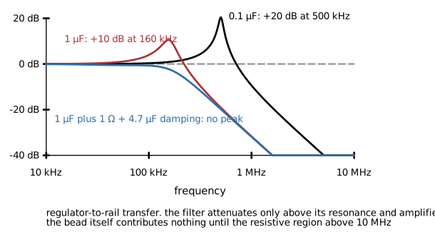 Figure 5. Transfer function from the regulator to the rail for the filter of Figure 4 with 0.1 µF, with 1 µF, and with 1 µF plus a damping branch. The undamped versions amplify at resonance.
Three consequences follow.
Ripple amplification. A switching regulator with a 500 kHz switching frequency feeding the 0.1 µF version delivers its ripple to the load amplified ten times. The bead, installed to clean the rail, has made it ten times worse at the one frequency where the noise was. The designer who then measures the rail sees the ripple and adds a second bead.
Load-step ringing. A step in load current excites the resonance. The rail rings at for cycles, dipping below and rising above its nominal value by an amount set by the step size and . A 100 mA step through 1 Ω of characteristic impedance is a 100 mV excursion on a 3.3 V rail, and an ADC or PLL on that rail sees it.
Interaction with the regulator loop. An LDO's output impedance rises with frequency as its loop gain falls, and the bead adds inductance in series with it. The combination can move the filter's resonance into the region where the LDO's phase margin is already small. LDO datasheets that show stability against output capacitance assume the capacitor is at the output pin, not behind an inductor.
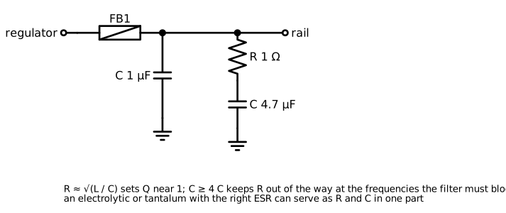 Figure 6. Damped rail filter. A resistor in series with a larger capacitor, in parallel with the bypass capacitor, sets the Q to about one without raising the impedance at high frequency.
The fix, when the bead stays, is damping. A resistor of about in series with a capacitor four or more times the bypass value, placed in parallel with it, brings the Q to about one and removes the peak. A tantalum or aluminum electrolytic whose ESR is near the required value serves as both parts. The damping branch adds nothing to the attenuation at high frequency, because the bypass capacitor still sets the impedance there.
Digital signals
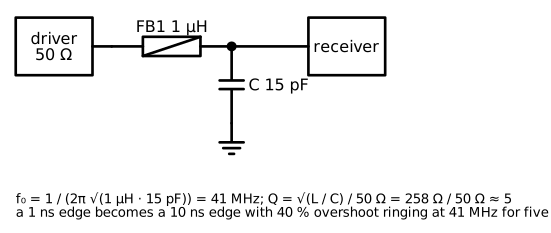 Figure 7. Bead in series with a logic signal. With the trace and input capacitance it forms a resonant circuit whose Q is set only by the driver's output impedance.
A bead in series with a digital line is an inductor in series with the driver, and the line's capacitance is the other half of a resonant circuit. With 1 µH and 15 pF the resonance is at 41 MHz and the Q, set by a 50 Ω driver, is about 5.
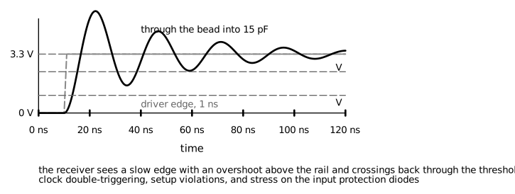 Figure 8. A 1 ns logic edge after passing through the bead of Figure 7. The receiver sees a slowed edge with overshoot and repeated crossings of the threshold band.
The receiver sees a 10 ns edge with 40 % overshoot ringing for five cycles. The overshoot exceeds the supply rail and conducts through the input protection diode. The ring crosses back through the input threshold band, which a clock input counts as extra edges and a data input samples as the wrong value. The edge rate that the bead was meant to slow for EMI reasons is now a 41 MHz oscillation that radiates at least as well as the original edge did.
A digital interface is specified by rise time, and the rise time is what the receiver needs for its setup and hold budget. Slowing it by design is done with a series resistor, which forms an RC with the line capacitance and has no resonance, and whose value is specified. A line that radiates does so because its return current has no low-impedance path back to the driver, which is a layout problem: the trace over a plane split, the connector without a ground pin beside the signal, or the cable without a shield or a common-mode choke. The common-mode choke is the part for that case, and it does not affect the differential signal.
The one place a bead in series with a signal is defensible is a slow signal on a long line leaving the board, such as a reset or an enable, where the edge rate is irrelevant and the line's capacitance is large enough to bring the resonance below the region where the bead is inductive. Even there a resistor does the same job predictably.
Ground
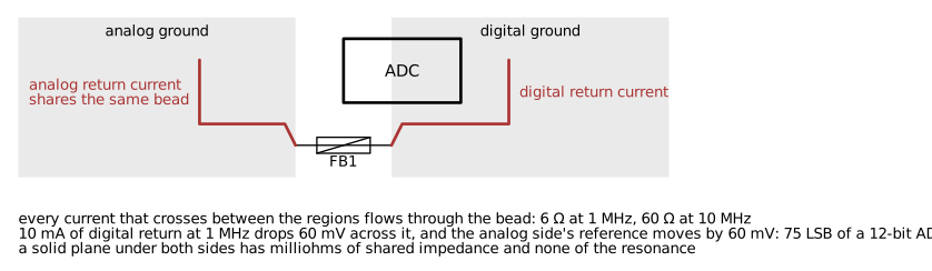 Figure 9. Two ground regions joined by a bead. Every current that crosses the split flows through the bead's impedance, and the drop appears as a shift between the two references.
The bead between an analog and a digital ground is the most durable misuse. The intent is to keep digital return currents out of the analog ground. The effect is to put 6 Ω at 1 MHz and 60 Ω at 10 MHz in the only path those currents have, so that every milliamp of return current develops millivolts across the bead, and the analog ground moves relative to the digital ground by that amount. An ADC with its analog reference on one side and its digital interface on the other has that voltage added to every conversion. At 10 mA and 1 MHz it is 60 mV, which is 75 LSB of a 12-bit converter on a 3.3 V reference.
The bead also forms a resonant circuit with the capacitance between the two ground regions and with every bypass capacitor that connects one region's rail to the other region's ground. The split has an impedance peak somewhere in the hundreds of kilohertz to a few megahertz, and at that frequency the two grounds are effectively disconnected.
A single solid ground plane has a shared impedance of milliohms and no resonance. Currents return under the trace that carried them, because that is the lowest inductance path, and analog and digital returns do not share copper unless the traces themselves cross. Separation is done by placement: the analog section in one area of the board with its own traces and its own decoupling, the digital section in another, and no signal crossing from one to the other except at the converter. The converter's ground pins connect to the one plane.
When a bead is the right part
A bead is a resistor that exists only at high frequency. That is a useful property in exactly one situation: a rail that carries a small, steady current, feeding a load that is sensitive to noise in the tens to hundreds of megahertz, where a series resistance at DC cannot be tolerated and a real inductor's Q would be a problem. A PLL supply on a large digital IC, drawing 20 mA and sensitive to the clock harmonics coupling in from the core supply, is the textbook case. So is the analog supply pin of a high-speed ADC, if the current is low and the noise is at the sampling clock's harmonics.
The conditions, all of which must hold:
- The noise to be removed is above the bead's crossover frequency, where it is resistive, and that has been established by measurement rather than assumed.
- The load current is small enough that the datasheet impedance still applies, which for most small beads means under a fifth of the rated current.
- The downstream capacitance has been chosen for a damped response, or a damping branch has been added, and the resonance has been placed away from the regulator's switching frequency and the load's transient content.
- The regulator feeding the bead is stable with the bead and capacitor as its load, which for an LDO means checking the datasheet's stability conditions with the added inductance.
- The rail has been measured with and without the bead, at the load, with a bandwidth that covers both the resonance and the noise, and the bead made it better.
A bead that satisfies these is a filter. A bead that does not is a resonator with an unknown inductance placed in a supply.
Alternatives
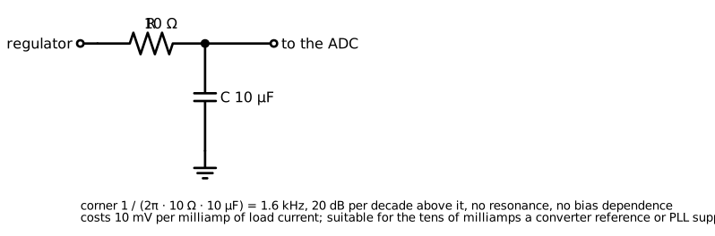 Figure 10. RC filter on a low-current rail. First order, fully characterized, no resonance, no bias dependence.
| Problem | What is usually done | What works |
|---|---|---|
| Regulator ripple on an analog rail | Bead and a capacitor | RC filter if the current allows, or an LC filter with a specified inductor and a damping branch, or an LDO post-regulator |
| Noise on an ADC or PLL supply pin | Bead from the digital rail | Bypass capacitor at the pin over a solid plane first; then a bead with damping and measured benefit, or an RC if the current is small |
| Digital edge too fast for the interface | Bead in series | Series resistor at the driver, sized for the line capacitance |
| Cable radiating | Beads in every signal | Common-mode choke on the cable, shield bonded at the connector, return pins beside signal pins |
| Analog and digital noise coupling | Ground split with a bead | One plane, partitioned placement, no traces crossing between regions except at the converter |
| Switching noise on a rail | Bead at the load | Input filter at the converter, tight power loop, decoupling at the switch; the noise is removed where it is generated |
| Clock harmonics on a supply | Bead | Decoupling at the clock driver and a controlled return path; the harmonics are on the rail because the driver's current loop is large |
An RC filter costs 10 mV per milliamp for 10 Ω, and a rail carrying 20 mA can afford that. Its corner is 1.6 kHz with 10 µF, it attenuates 20 dB per decade above it, and both elements are specified to 1 % over temperature and bias. An LC filter with a real inductor has a specified inductance, a specified saturation current, and a datasheet self-resonance, so its resonance can be calculated and damped by design rather than discovered.
Measuring the situation
Before a bead is added, the noise it is meant to remove should be characterized: its frequency, its amplitude, and its source. A spectrum analyzer or a scope FFT on the rail, with a probe grounded at the load, gives the first two. The third comes from correlating the noise with the switching frequency, the clock, or the bus activity.
After a bead is added, the rail should be measured at the load with the load running, with a bandwidth covering both the resonance and the noise band. A load step should be applied and the rail's response recorded. An impedance analyzer, or a network analyzer with a series injection, can measure the transfer function directly.
A bead whose benefit cannot be shown on the bench is not doing anything the bypass capacitor was not already doing, and may be doing harm that the measurement has not yet found.
Design errors
- Inductance estimated from the 100 MHz impedance. The part is resistive there, and the inductance is lower than at that point. Correction: use the impedance curve at a frequency where the phase is still near 90°, typically 1 to 10 MHz.
- Resonance calculated with the nominal capacitor value. A 1 µF ceramic at 3.3 V on a 0402 footprint may be 0.4 µF, which moves the resonance up by 60 % and raises the Q. Correction: use the capacitance at bias, from the manufacturer's curve.
- Damping omitted because the bead "is resistive". Its resistance at the resonance frequency is the DC resistance, a fraction of an ohm. Correction: damping branch or an RC filter.
- Bead selected by impedance alone. Two 600 Ω beads with different crossover frequencies are different filters. Correction: compare the full impedance curves, and record the vendor part number as a design constraint.
- Bead on the output of an LDO with a ceramic load. The LDO's stability was specified for a capacitor at its pin. Correction: the bypass capacitor stays at the LDO output; the bead and its own capacitor follow, with damping.
- Ground split with a bead under a mixed-signal converter. Correction: one plane, placement, and the converter's ground pins on it.
- Bead in a signal line to pass a radiated emissions test. The ring at the LC resonance radiates too. Correction: fix the return path, add a common-mode choke at the cable, or use a series resistor if the edge must be slowed.
- Bead carrying the rated current. Impedance is a fraction of the datasheet value. Correction: derate to a fifth of the rated current, or use a larger part, or use an inductor with a specified saturation current.
Limitations of this document
- The bead model in the figures is a single representative part. Real parts vary in every parameter, and the crossover frequency in particular ranges over a decade between products with the same nominal impedance.
- Q and peaking values are computed with a fixed 0.3 Ω of damping. Source impedance, capacitor ESR, and trace resistance change the result, usually by less than a factor of two.
- The digital edge example uses a lumped trace capacitance. Long traces behave as transmission lines, and the bead's effect then depends on the line impedance as well.