Splitting Ground Planes
noteWhy a split ground plane is almost never the right answer: where return current actually flows, what happens when a trace crosses a gap, how splits create crosstalk, reflections, and radiated emissions, the one case where two grounds are required, and how to get the isolation people want from a split by placement on a single plane instead.
Scope: the ground return in multilayer boards carrying mixed analog, digital, and switching power circuits. The note follows the argument made by Eric Bogatin, Rick Hartley, and Zachariah Peterson, which is the argument from physics: a signal and its return current are one circuit, the return follows the signal, and cutting the copper the return needs is the cause of the problems the cut was meant to prevent. Two-layer boards and chassis grounding are covered where they differ.
Common errors
- Splitting the plane into analog and digital regions. Any trace that crosses the split, and there is always one, sends its return current around the end of the gap. The loop that results is the largest inductance on the board.
- Treating ground as a reference rather than a return. "Ground" on a schematic is a node. On a board it is a conductor carrying every return current, and its job is to carry each one directly under the trace that sourced it.
- Placing a bead or a zero-ohm link across the split. The link is the only path for every crossing return current, so every crossing circuit shares its impedance. See the ferrite bead note for the numbers.
- Routing over a gap in the reference plane because the gap is a power plane split, a slot for a connector, or a cutout under a transformer. The reference plane under a signal must be continuous for the length of the signal.
- Assuming low-frequency signals are exempt. The edges of a 1 kHz logic signal contain energy to hundreds of megahertz. The return current for the edge behaves as a high-frequency current regardless of the repetition rate.
- Following a reference design's split without its reason. Some reference designs split for galvanic isolation; some carry a split from an older revision that never worked well; some have a split because the application note's author was repeating advice from the era of two-layer boards.
- Stitching capacitors as a repair. A capacitor across a gap gives the return current a path only at frequencies where its impedance is low, adds an inductive loop through its pads and vias, and does nothing for the low-frequency part of the return.
Where return current flows
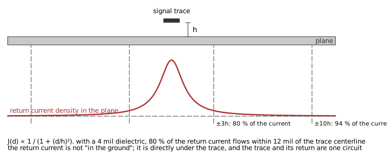 Figure 1. Return current density in a plane under a signal trace at height h. The distribution is proportional to 1 over 1 plus the square of the distance-to-height ratio; most of the current is within a few trace heights of the centerline.
A signal trace over a plane is a transmission line. The current that leaves the driver on the trace returns on the plane, and at any frequency above a few tens of kilohertz it returns directly beneath the trace, because that is the path that encloses the least area and therefore has the least inductance. The current density in the plane at lateral distance from the trace centerline, with the trace at height above the plane, is
The fraction of the return current within of the centerline is : 80 % within three trace heights, 94 % within ten. With a 4 mil dielectric, 80 % of the return current flows within a 24 mil wide strip under the trace. The plane's other square inches carry almost nothing for that signal.
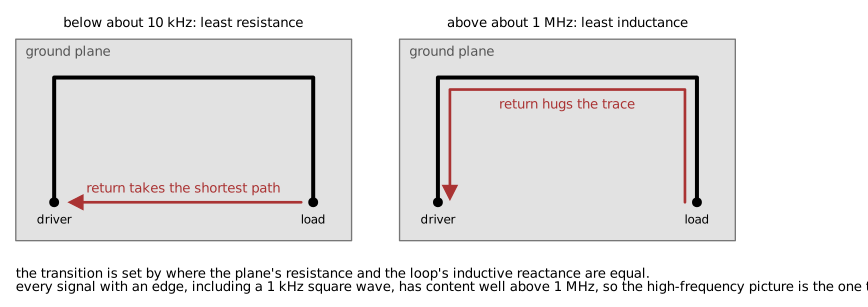 Figure 2. The same trace at two frequencies. At low frequency the return takes the shortest path through the plane; above about 1 MHz it follows the trace. The transition happens where inductive reactance overtakes resistance.
At DC the return current spreads across the whole plane, following the path of least resistance, which is the straight line between the load and the driver. As frequency rises the inductive reactance of a wide loop grows while the resistance of the plane does not, and the current migrates to the path of least inductance, which is under the trace. The transition is complete by about 1 MHz for typical plane geometries and begins around 10 kHz. Every logic edge, every switching transition, and every clock harmonic is well above this, so the high-frequency picture is the operative one for every signal that has an edge.
Two consequences follow. First, the plane under a trace is part of that trace's circuit and nothing else's; two traces a few hundred mils apart on the same plane do not share return current. Second, a solid plane already provides the separation that a split is supposed to provide, and provides it by physics rather than by copper removal.
What happens at a gap
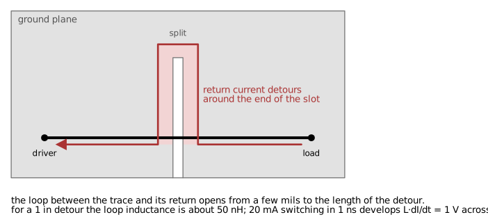 Figure 3. A trace crossing a slot in the plane. The return current cannot follow the trace and detours around the end of the slot, opening a loop whose size is the detour.
A trace that crosses a gap in its reference plane has no return path beneath it for the length of the gap. The return current goes around the end of the gap, and the loop between the signal and its return grows from the dielectric thickness, a few mils, to the length of the detour, which can be inches. The consequences are the consequences of loop inductance.
Ground bounce. The detour has inductance , and the signal's edge drives a current change through it. For a 1 inch detour the loop inductance is on the order of 50 nH, and a 20 mA edge in 1 ns produces
across the slot. The two sides of the plane are at different potentials by a volt for the duration of the edge. Every component referenced to one side sees the other side move.
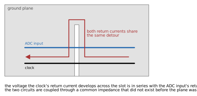 Figure 4. Two traces crossing the same slot. Their return currents share the detour, and the voltage one develops across it appears in series with the other.
Crosstalk through common impedance. Every trace that crosses the same gap shares the same detour. The voltage that a clock's return current develops across the slot is in series with the return path of an ADC input crossing the same slot, and it appears at the ADC's input as noise synchronous with the clock. Two circuits that shared nothing on a solid plane are coupled through an impedance the split created. This is the mechanism that the split was supposed to prevent, produced by the split.
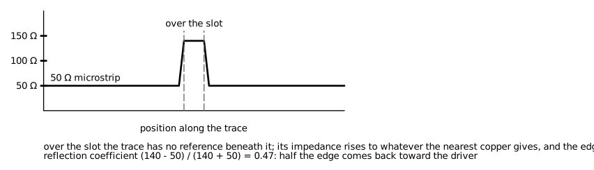 Figure 5. Impedance along a trace that crosses a slot. Over the slot the trace has no reference beneath it and its impedance rises; the mismatch reflects part of the edge.
Reflections. A 50 Ω microstrip is 50 Ω because of the plane beneath it. Over the gap it is a wire with a distant reference and an impedance of 100 to 200 Ω. The mismatch reflects a portion of the edge back toward the driver, , about 0.5 for a 150 Ω gap impedance. The reflection appears as a step or a glitch on the edge, and on a bus with several crossings the reflections add.
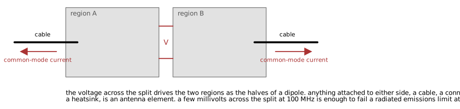 Figure 6. The two regions of a split plane, driven by the voltage across the gap, form a dipole. Cables and other conductors attached to either side carry common-mode current and radiate.
Radiated emissions. The voltage across the slot drives the two halves of the plane as the two arms of a dipole antenna, and every conductor attached to either half, a cable, a connector shell, a heatsink, becomes part of it. The slot itself radiates as a slot antenna, efficiently when its length approaches a quarter wavelength, which for a 2 inch slot is about 1.5 GHz, and measurably at lower frequencies. Common-mode current of a few microamps on a cable is enough to fail a Class B radiated emissions limit at 3 m, and a few millivolts across a split at 100 MHz drives that much current into a meter of cable. The board that passes with a solid plane and fails with a split is a routine outcome in an EMC lab.
Power integrity. A power trace or plane that crosses a ground split has the same detour in its return, so the supply's transient response acquires the inductance of the detour. The rail rings on every load step, and the decoupling capacitors on the far side of the split are less effective because the loop through them is larger.
The split does not do what it is meant to do
The intent behind an analog-digital split is to keep digital return currents out of the analog ground. On a solid plane they already are. Digital return currents flow under digital traces, within a few trace heights of them, and do not enter the region under the analog traces unless a digital trace is routed there. Keeping digital currents out of the analog area is done by keeping digital traces out of the analog area, which is a placement and routing decision, not a copper decision.
The intent behind a split around a switching converter is to contain its noise. The converter's noise is carried by its high loops, which are the input capacitor, the switch, and the diode or synchronous switch, and by the switch node's into whatever capacitance faces it. Both are contained by a tight layout of those loops over a solid plane and by keeping other traces away from the switch node. A split under the converter forces its return currents around the split's ends, enlarges its loops, and increases the noise.
The intent behind a split for a sensitive front end is to keep the reference of the amplifier's input stage clean. The front end's reference is clean when its return currents are small and local, which they are when its components are placed together and its decoupling returns to the plane beside them, and when no large current is routed through the copper beneath it. The split adds a slot next to the front end that radiates into it.
In each case the split addresses a problem that a solid plane with correct placement does not have, and creates the problems described above.
Partition by placement
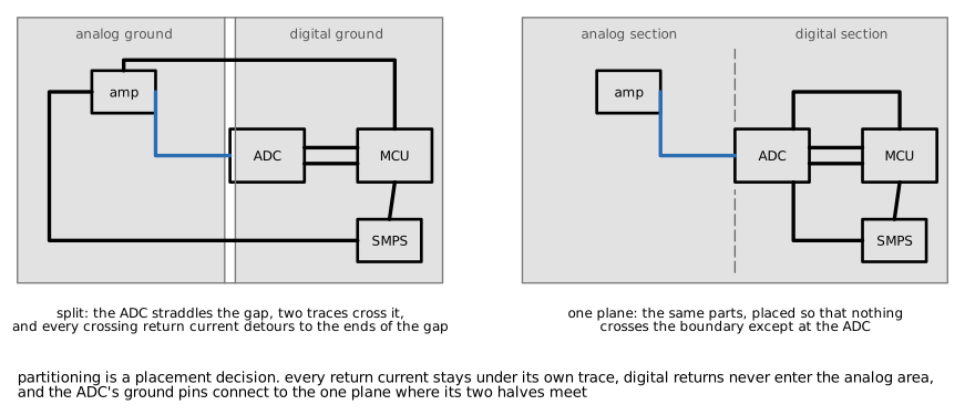 Figure 7. The same circuit on a split plane and on a single plane. On the single plane the parts are placed so that only the converter sits at the boundary and no trace crosses it.
The approach that works is partitioning. The board is divided into regions by function, analog input, converter, digital processing, switching power, and the parts of each function are placed within its region. Traces stay within their region. The one component that must belong to two regions, the ADC or DAC, is placed at the boundary with its analog pins facing the analog region and its digital pins facing the digital region. Its ground pins connect to the one plane. The boundary is a line on the placement drawing, not a cut in the copper.
Rules for the partition:
- No trace crosses from one region to another except the converter's own pins. A control signal from the processor to an analog switch is routed to the boundary and then within the analog region, or the analog switch is placed at the boundary.
- Return current for every trace is under that trace. Check the reference plane under each route for continuity: no slots from connector cutouts, no plane splits from a power plane serving as reference, no via fields that fragment the copper.
- Decoupling returns locally. Each device's bypass capacitors connect to the plane beside the device, so its return currents close within its own footprint.
- The switching converter's loops are tight and its switch node small. The converter is in its own region with the noisy nodes away from the region boundary.
- Chassis and cable shields connect to the plane at the connector, in one place, so that the plane and the chassis are at the same potential at the point where cables leave.
The result is a board on which the analog and digital sections are separated by distance and by the physics of return current, with a plane that is one conductor everywhere.
The one legitimate split
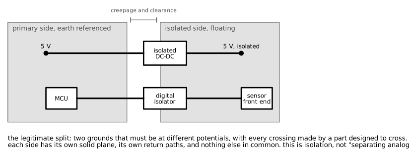 Figure 8. Galvanic isolation. Two grounds that must be at different potentials, each with its own solid plane, joined only by parts designed to cross the barrier.
A ground is split when two circuits must be at different potentials: an isolated power supply, a mains-connected primary and a user-accessible secondary, a floating measurement front end, an isolated communication interface. These are two grounds, not one ground divided, and the requirement comes from safety or from a real potential difference, not from noise.
The split is designed as follows. Each side has its own solid plane and its own complete return paths. The gap between them is sized for the required creepage and clearance, and nothing crosses it except parts built to cross it: an isolated converter or transformer for power, a digital isolator, optocoupler, or isolation amplifier for signals. No trace crosses the gap. No plane on any layer bridges it. A safety-rated capacitor may connect the two sides for common-mode EMI, placed at the transformer, and it is the only connection.
A split of this kind has none of the problems above because no return current attempts to cross it. Every signal that passes from one side to the other is converted, in the isolator, into a signal whose return path is on the far side.
Two-layer boards
A two-layer board has no solid plane to split. The same physics applies: return current wants to be under the trace, and the bottom layer should be as continuous a ground as the routing allows. Ground pours on both layers stitched together with vias, no traces routed across the ground pour on the bottom layer where a signal runs above, and signal traces on the top layer routed so that the copper beneath them is unbroken for their whole length. A two-layer board that must carry a switching converter and an ADC benefits more from moving to four layers than from any grounding trick.
Measuring the situation
A near-field probe over the plane, with the board running, finds the slots and the return-path detours by their magnetic field. A trace's return path can be confirmed with a TDR or a VNA: a gap in the reference shows as an impedance step at the location of the gap. Crosstalk across a slot is measured directly with two probes, one on the aggressor edge and one on the victim, with the aggressor's return forced across the slot. Radiated emissions, before and after a plane change, are the final measurement and the one that decides.
Design errors
- Ground plane split under a mixed-signal converter. Correction: one plane, converter at the partition boundary, ground pins to the plane.
- Signal routed over a power plane split on a layer that uses the power plane as its reference. Correction: route over ground, or make the power plane continuous under the trace.
- Slot from a row of connector pins or a via field across a signal route. Correction: route around the slot, or move the connector so that traces cross it where the copper is continuous.
- Stitching capacitor across a split as the return path. Correction: remove the split; if the split is for isolation, the signal goes through an isolator.
- Ferrite bead joining two ground regions. Correction: as above.
- Star ground on a multilayer board. The star point is a single connection between regions, and every return current that would cross between them concentrates in it. Correction: one plane; the star belongs to single-point grounding of cables and chassis, not to on-board returns.
- Reference plane two or more dielectrics away from the signal layer. The return current is far from the trace and the loop is large. Correction: a plane adjacent to every signal layer.
- Converter placed astride a plane split for "noise containment". Correction: converter in its own region on the solid plane, with tight loops.
Limitations of this document
- The loop inductance figure is an order-of-magnitude estimate for a 1 in detour with typical geometry. Exact values depend on the slot length, the trace height, and the return path width.
- The impedance over a gap depends on what copper is nearest. 150 Ω is representative of a trace passing over a slot with a plane on a farther layer; with no other copper the impedance is higher.
- Emissions figures are order-of-magnitude. Whether a given split fails a given limit depends on the cable, the enclosure, the spectrum of the crossing signals, and the test distance.
References
- Zachariah Peterson, Altium Academy: Never Cross a Ground Plane Gap in High Speed PCB Design, What is the Electrical Return Path in a PCB?, Should You Use Star Grounding for Analog and Digital Ground Separation?, Crosstalk in Mixed-Signal PCB Traces and Ground Planes.
- Rick Hartley, "How to Achieve Proper Grounding" (Altium, 2019 talk), and design recommendations summarized by Sierra Circuits.
- Eric Bogatin, Ground Rules for Grounding, Signal Integrity Journal, and Return Current Path with Robert Feranec.
- Howard Johnson, High-Speed Digital Design, equation 5.2 for the return current distribution, and Return Current in a Plane.
- Signal Integrity Journal, The Case for Split Ground Planes, for the narrow parallel-gap case and its measured 0.4 to 0.25 nH mutual inductance change.