Noise in Circuits
noteWhere electrical noise comes from and how it gets into a circuit: intrinsic noise in resistors and amplifiers, the four coupling paths, common mode versus differential mode, switching converters and fast edges as sources, and the layout, grounding, shielding, and front-end practices that keep noise out of a sensitive measurement.
Scope: noise in analog, mixed-signal, and power electronics at the board and cable level. The note separates noise that a circuit generates internally from noise that is coupled in from elsewhere, gives the mechanism and a number for each, and then covers the defenses in the order they should be applied: source, path, and receiver. Radio-frequency circuit design and audio-specific practice are outside the scope. The ground plane and ferrite bead notes cover two of the topics here in more depth.
Common errors
- Treating all noise as one thing. Thermal noise in a resistor, a switching converter's edges coupling into an input, and 60 Hz hum from a ground loop are three different problems with three different fixes. Measuring which one is present comes before any fix.
- Filtering at the receiver first. A filter removes noise that is already in the signal band only by removing signal. Noise is removed most cheaply at its source and along its path; the receiver's filter is the last step.
- Adding decoupling capacitors without regard to loop area. A capacitor a centimeter from the pin, with the return routed around the board, has tens of nanohenries in its loop and does nothing above a few megahertz.
- Running a sensitive trace past a switch node. A picofarad of stray capacitance and 10 V/ns is 10 mA injected at every edge.
- Grounding a cable shield with a pigtail. The shield's current comes inside on a wire whose inductance defeats the shield above a few megahertz.
- Splitting ground planes for noise. The split creates a shared return impedance where none existed and a slot that radiates.
- Ignoring common mode because the receiver is differential. Common-mode rejection falls with frequency and is set by the balance of the whole path, not by the amplifier's datasheet figure.
- Looking at noise with the wrong probe. A 15 cm ground clip adds its own 130 MHz ringing to every measurement and a 10:1 probe adds ten times the scope's noise floor to every reading.
Two kinds of noise
Intrinsic noise is generated by the components of the circuit and is random. Interference is generated somewhere else and coupled in, and it is deterministic: it has the frequency, edge rate, and timing of its source. The distinction decides the approach. Intrinsic noise is reduced by the choice of components, impedances, and bandwidth. Interference is reduced by controlling the coupling path.
The two are told apart on the bench. Interference correlates with something: it appears at the switching frequency, at the clock rate, at 50 or 60 Hz, or when a particular subsystem is running. Intrinsic noise is white or 1/f, does not change when other parts of the system are turned off, and scales with the square root of bandwidth.
Intrinsic noise
Every resistance generates thermal noise with a voltage density of
which is 4 nV/√Hz for 1 kΩ and 13 nV/√Hz for 10 kΩ at room temperature. Every current crossing a junction generates shot noise, , and every amplifier and most resistors add 1/f noise below a corner frequency that ranges from under 1 Hz for good bipolar parts to kilohertz for CMOS and for carbon composition resistors.
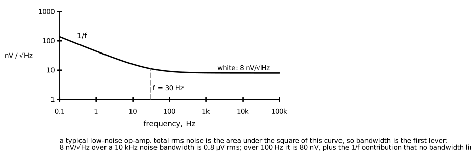 Figure 1. Voltage noise density of a low-noise op-amp. A 1/f region below the corner frequency and a white region above it. Total noise is the integral of the square of this curve over the bandwidth.
The total rms noise is the noise density integrated over the noise bandwidth. For white noise that is the density times the square root of the bandwidth, and the noise bandwidth of a first-order low-pass filter is 1.57 times its 3 dB frequency. Sources add as the square root of the sum of squares, which has a practical consequence: the largest source dominates, and reducing any source that is under a third of the largest changes the total by less than 5 %.
| Source | Density | 1 kΩ, 10 kHz noise bandwidth | Reduced by |
|---|---|---|---|
| Resistor, thermal | 0.4 µV rms | Lower resistance, lower temperature, narrower bandwidth | |
| Amplifier voltage noise | datasheet , 1 to 50 nV/√Hz | 0.1 to 5 µV rms | Part selection; bipolar input for low source impedance |
| Amplifier current noise into | , 0.1 fA to 2 pA/√Hz | negligible to 2 µV rms | JFET or CMOS input for high source impedance |
| 1/f | rises below | depends on and the low-frequency limit | Chopper or zero-drift amplifiers; AC excitation and demodulation |
| Shot noise in a diode or transistor | 57 pA rms at 1 mA | Higher current for a given signal; irrelevant in most op-amp circuits | |
| Quantization | LSB/√12 | 0.23 mV rms at 12 bits, 3.3 V | More bits, oversampling with dither |
The rule for a low-noise front end is to make the signal source's impedance the dominant resistance, choose an amplifier whose is below the source's thermal noise and whose is below both, and set the bandwidth to what the measurement needs and no more.
How noise gets in
Interference reaches a victim circuit by four paths. Each has a governing equation, and the equation names the lever.
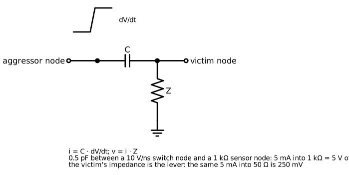 Figure 2. Capacitive coupling. A fast-moving voltage on one node drives current through the stray capacitance into any node nearby, and the victim's impedance turns that current into a voltage.
Capacitive. Current flows through the stray capacitance between an aggressor node and the victim. The injected current develops a voltage across whatever impedance the victim node presents. With 0.5 pF between a 10 V/ns switch node and a 1 kΩ sensor node, 5 mA flows and the node moves by 5 V. The levers are the capacitance, which is set by area and distance, the edge rate, and the victim's impedance. A low-impedance node is nearly immune to capacitive coupling; a high-impedance node is a receiver for it.
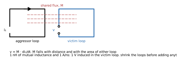 Figure 3. Inductive coupling. A changing current in one loop produces flux through a nearby loop and induces a voltage in it proportional to the mutual inductance.
Inductive. A changing current in one loop induces in another. The mutual inductance depends on the areas of both loops and their separation. With 1 nH of mutual inductance and 1 A/ns, the victim sees 1 V. Unlike capacitive coupling, inductive coupling does not care about the victim's impedance; it is a voltage in series with the victim loop. The levers are loop area, on both sides, and distance. Inductive coupling is the dominant path from a switching converter's hot loop into anything within a few centimeters.
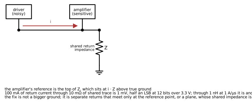 Figure 4. Conductive coupling. Two circuits that share a return conductor share its impedance, and one circuit's return current appears as a voltage in the other's reference.
Conductive. Two circuits that share a length of conductor share its impedance. The return current of one develops a voltage across it that the other sees in its reference. This is the mechanism of ground noise on a board and of hum in a ground loop. 100 mA of digital return current through 10 mΩ of shared trace is 1 mV; the same current with 1 A/µs of edge through 1 nH is another 1 mV. The lever is the shared impedance, which is why a plane, with microohms of shared impedance, beats any arrangement of traces.
Radiated. At distances beyond a wavelength divided by 2π, the fields have detached from their sources and propagate as waves. On a board, at frequencies below a gigahertz, that distance is larger than the board, so on-board coupling is one of the three near-field mechanisms above. Radiation matters at the cables, which are long enough to be antennas at tens of megahertz, and at the enclosure. A cable carrying a few microamps of common-mode current at 100 MHz radiates enough to fail a Class B emissions limit at 3 m.
Common mode and differential mode
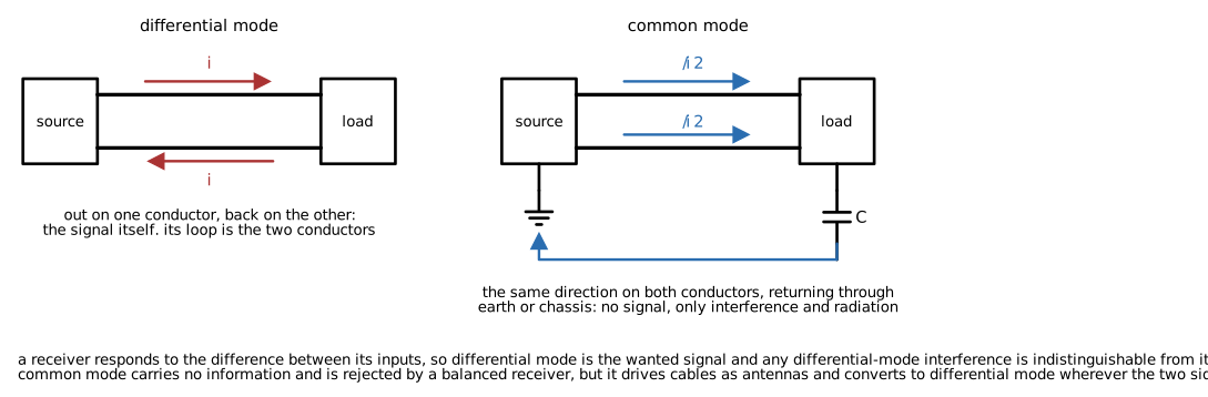 Figure 5. Differential-mode current flows out on one conductor and back on the other; it is the signal. Common-mode current flows the same direction on both and returns through stray capacitance or earth; it carries no signal.
Any pair of conductors carries two independent currents. The differential-mode current flows out on one conductor and back on the other. It is the signal, and its loop is the space between the two conductors. The common-mode current flows in the same direction on both conductors and returns through some other path: the chassis, the earth, or the stray capacitance between the cable and its surroundings. It carries no information.
The two modes have different consequences. Differential-mode interference is indistinguishable from the signal, because it is on the same conductors in the same sense, and only filtering by frequency separates them. Common-mode interference is rejected by any receiver that responds only to the difference between its inputs, which is what a differential amplifier, a transformer, or a balanced line does. But common mode has two ways of doing harm anyway.
It radiates. A cable with a common-mode current is a monopole antenna driven against the chassis. The differential-mode current of the same magnitude radiates very little, because the two conductors carry it in opposite directions and their fields cancel at any distance larger than their spacing. Emissions failures from cables are almost always common mode.
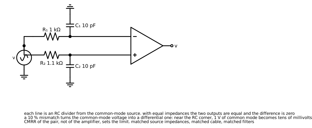 Figure 6. Mode conversion. A common-mode voltage driving a pair with unequal impedances produces a differential voltage at the receiver, no matter how good the receiver's own rejection is.
It converts to differential mode wherever the two conductors are not identical. If the two lines have different source impedances, different capacitances to ground, or different filter components, the common-mode voltage divides differently on each and the difference is a differential-mode signal. A 10 % mismatch in a pair of RC filters converts 1 V of common mode into tens of millivolts of differential mode near the filter corner. The common-mode rejection of a channel is therefore set by its balance, and the amplifier's CMRR is only the last stage of it.
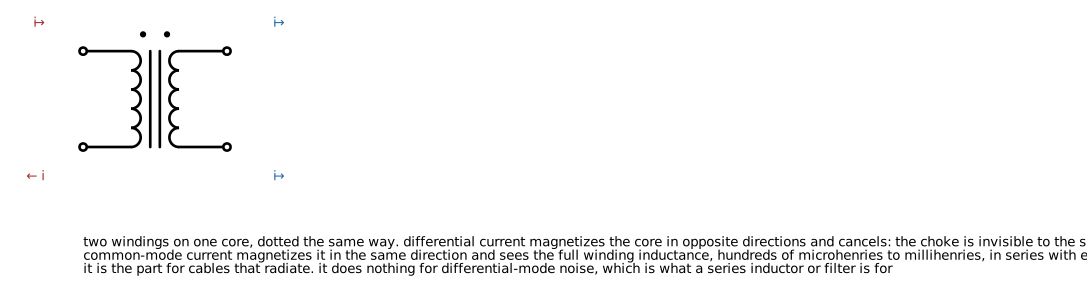 Figure 7. Common-mode choke. Two windings on one core; differential current cancels in the core and passes, common-mode current sees the full inductance.
The common-mode choke is the component built for this distinction. Both conductors pass through the same core, wound so that the differential current's flux cancels and the common-mode current's flux adds. The signal sees a few microhenries of leakage inductance; the common-mode current sees hundreds of microhenries to millihenries. It is the correct part for a cable that radiates and does nothing for differential noise, which is handled by ordinary filtering.
Sources
Switching converters. A converter has two noisy quantities: the switch node, which slews through the input voltage in a few nanoseconds, and the hot-loop current, which steps between zero and the inductor current at each edge. The switch node couples capacitively into everything with a view of it. The hot loop couples inductively into every loop within a few centimeters and puts an spike on the converter's own ground and input.
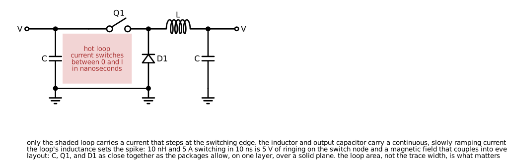 Figure 8. Buck converter with the hot loop shaded. Only the input capacitor, the switch, and the diode carry the current that steps at the switching edge. The inductor and output capacitor carry a continuous current.
The hot loop is the input capacitor, the switch, and the freewheeling diode or synchronous switch. The inductor and the output capacitor are not in it; their current ramps but does not step. The loop's inductance sets the spike amplitude: 10 nH of loop inductance and 5 A switching in 10 ns is 5 V across the loop, which appears as ringing on the switch node, as noise on the input rail, and as a magnetic field around the loop. The layout rule is to make that loop as small as the packages allow, on one layer, over an unbroken plane.
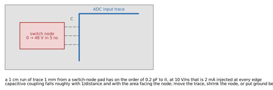 Figure 9. Switch node next to a sensitive trace. A centimeter of trace a millimeter from the node has a fraction of a picofarad to it, which at 10 V/ns injects milliamps at every edge.
Digital edges. A logic edge's spectrum extends to about : 500 MHz for a 1 ns edge, regardless of the clock rate. Every logic output, every clock, and every bus is a source at those frequencies, and the current that flows at each edge, from the supply through the output into the load capacitance and back, is a small hot loop. A 3.3 V driver charging 20 pF in 1 ns draws 66 mA for that nanosecond.
Motor drives, relays, and solenoids. Inductive loads interrupted without a clamp produce hundreds of volts of kickback and arcs at the contacts, which radiate to tens of megahertz. A flyback diode or an RC snubber across the load, at the load, removes the source.
Mains. 50 or 60 Hz enters by conductive coupling through ground loops and by capacitive coupling from wiring into high-impedance nodes. Its harmonics, from rectifier loads on the same circuit, extend to a few kilohertz. An unterminated 1 MΩ input a meter from a mains cable picks up tens of millivolts.
Radio-frequency sources. Cellular and Wi-Fi radios within a meter of a board deliver volts per meter. The field itself is above the bandwidth of most analog circuits, but the input stage of any amplifier is a rectifier for it, and the rectified envelope appears as a DC shift or a low-frequency signal that no downstream filter removes. This is the mechanism behind a sensor reading that changes when a phone is nearby.
Electrostatic discharge. A discharge to a connector or an enclosure is a current pulse of amperes with a 1 ns rise, and its field couples into everything nearby. The protection device at the port limits the voltage; the layout of the path from the port to the chassis determines whether the pulse's field reaches the rest of the board.
Layout
The near-field mechanisms are governed by geometry, so layout is the primary defense. The rules, in order of leverage:
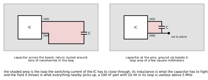 Figure 10. Decoupling capacitor loop area. The loop through the IC's supply and ground pins and the capacitor must be small, because its inductance limits the capacitor and its field radiates.
- Minimize the area of every loop that carries a changing current. The hot loop of a converter, the gate drive loop, the decoupling loop of every digital IC, and the signal-and-return loop of every trace. Inductance is proportional to loop area, and so are both the voltage and the field radiated. A plane adjacent to every signal and power layer makes the return path automatic and keeps the loop area to the trace's height above the plane.
- Keep aggressors and victims apart. Capacitive coupling falls roughly as the inverse of distance for a trace beside a node and inductive coupling between small loops falls as the inverse cube. The switching section, the digital section, and the analog front end go in different areas of the board, and the front end is farthest from the switch node.
- Keep the reference plane continuous. No splits, no slots from via fields or connector cutouts under sensitive or fast traces, no signals crossing the boundary between a ground plane and a power plane used as a reference.
- Route sensitive signals short and low. A high-impedance node is an antenna for capacitive coupling in proportion to its length and impedance. Keep it short, keep the impedance as low as the source allows, and route it on a layer adjacent to ground.
- Cross at right angles. Where a sensitive trace must cross an aggressor on another layer, cross at 90° to minimize the overlap area and therefore the capacitance.
- Guard high-impedance nodes. A ground trace on both sides of a high-impedance input, and a ground pour on the layer beneath it, intercept capacitive coupling before it reaches the node. For picoampere inputs, a guard driven at the input's own potential removes leakage as well.
- Place decoupling by loop, not by count. One capacitor at the pin with a via to the plane beside it does more than five capacitors along a bus.
Grounding
Ground is the return path for every current on the board, and it is the reference against which every voltage is measured. Both jobs are done by the same copper, and noise on the ground is the direct result of return currents flowing through impedance that a reference shares.
One plane. A solid plane has a shared impedance of microohms and gives every high-frequency return current a path directly under its trace. It solves conductive coupling on the board better than any topology of traces. Star grounds, single-point grounds, and split planes are attempts to control return paths by hand, and above a few hundred kilohertz they lose to the physics that puts the return under the trace regardless.
Single-point below, multipoint above. At audio and low frequencies, where the inductance of a return path is not yet its dominant impedance, a single-point ground avoids loops and the hum they carry. Above about a megahertz, return current must be allowed to take the shortest path, which means many connections to the plane and to the chassis. The two regimes coexist in most systems: a single connection between the board's plane and the chassis at the connector, and multipoint connections everywhere else.
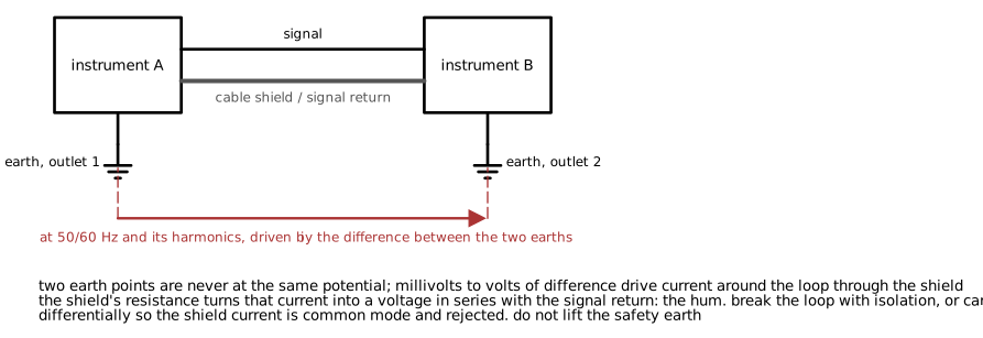 Figure 11. Ground loop. Two instruments earthed at different outlets and connected by a cable form a loop that carries mains-frequency current through the cable's shield or return.
Ground loops. Two pieces of equipment earthed at different points are at slightly different potentials, and a cable connecting them completes a loop that carries current at the mains frequency and its harmonics. The current develops a voltage across the cable's return conductor, and that voltage is in series with the signal. The remedies, in order of preference: carry the signal differentially so the loop voltage is common mode and rejected; break the loop with a transformer, an optocoupler, or an isolated interface; connect the shield so that it does not carry the signal return. Lifting the safety earth is not a remedy.
Chassis. The board's plane and the enclosure are bonded at the connectors, where cables enter, so that the cable shields' currents flow onto the chassis and not into the board. A board grounded to the chassis at one corner and carrying its connectors at the other corner routes every shield current across the board's plane.
Shielding
A shield is a conductor between a source and a victim. It works differently for the two fields.
Electric field. A grounded conductor between the source and the victim terminates the field lines that would have reached the victim, and the stray capacitance becomes capacitance to the shield instead. Any conductor thick enough to be continuous works; a thin foil or a plated plastic is enough. The shield must be connected to the circuit's reference, and its connection must be low impedance at the frequency of interest, or the shield itself becomes a coupling node.
Magnetic field. At high frequency, a conductive shield excludes the field by eddy currents, and its effectiveness depends on conductivity and thickness relative to skin depth. At low frequency, only a high-permeability material, mu-metal or steel, diverts the flux, and a copper shield does nothing. The practical alternative at low frequency is loop area: a twisted pair has a loop area of nearly zero and cancels magnetic pickup better than any shield.
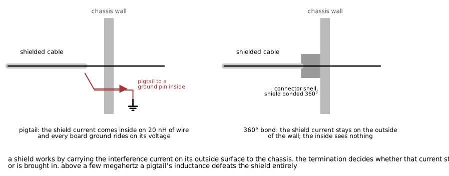 Figure 12. Cable shield termination. A pigtail brings the shield current inside the enclosure on an inductive wire; a 360° bond at the connector keeps it on the outside.
Termination. The shield's job is to carry the interference current, from whatever field the cable sits in, to the chassis without letting it into the circuit. A 360° connection between the shield and the connector shell, and the shell and the chassis, does that. A pigtail, a few centimeters of wire from the shield's drain wire to a ground pin, has 20 nH or more of inductance and puts the shield's entire current through that inductance inside the enclosure, where the voltage it develops is in the circuit's ground. Above a few megahertz a pigtail defeats the shield.
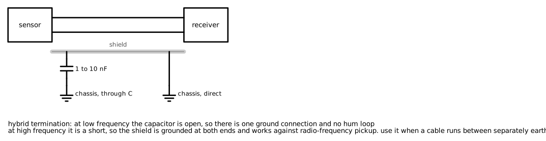 Figure 13. Hybrid shield grounding. Direct at one end, through a capacitor at the other: a single connection at mains frequency, both ends at radio frequency.
One end or both. A shield grounded at both ends is a ground loop at mains frequency and a shield at radio frequency. A shield grounded at one end is not a loop but does not shield against radio-frequency fields, because it cannot carry their current. The hybrid termination, direct at one end and through a capacitor of 1 to 10 nF at the other, gives one connection at low frequency and two at high frequency, and is the choice for cables between separately earthed equipment.
Enclosures. A metal enclosure is a shield with holes. Every seam, slot, vent, and display cutout leaks, and a slot leaks most when its longest dimension approaches half a wavelength: 15 cm at 1 GHz. Gaskets, overlapping seams, many fasteners, and honeycomb vents keep the apertures electrically small. Cables that pass through the wall carry the outside onto the inside unless their shields are bonded at the wall.
Protecting the sensitive end
After the source and the path have been dealt with, the receiver is designed to reject what is left.
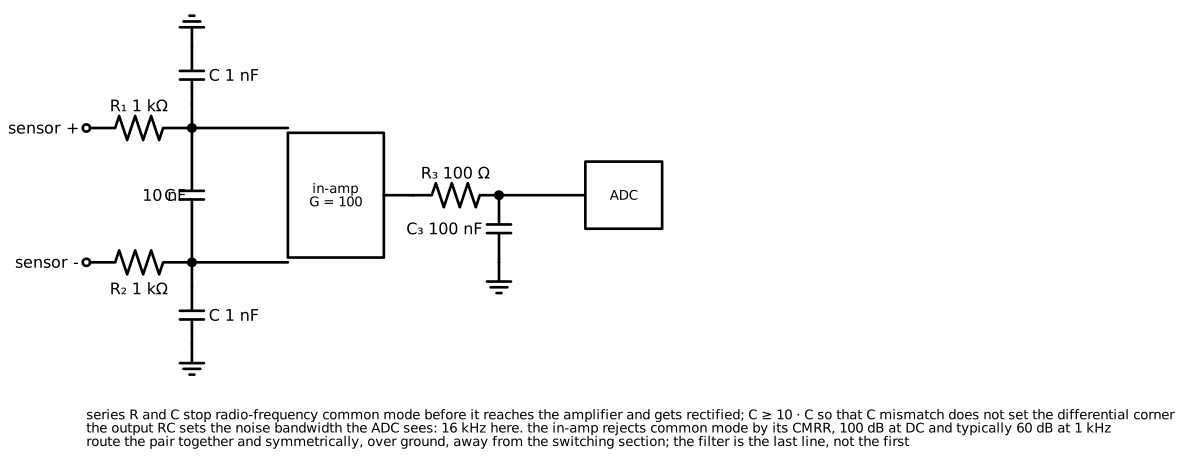 Figure 14. Instrumentation amplifier front end with common-mode and differential-mode filtering, an output filter that sets the noise bandwidth, and matched components on both lines.
- Differential input with matched impedances on both lines. It rejects common mode at low frequency by the amplifier's CMRR and at high frequency by the balance of the filter and cable.
- Radio-frequency filter ahead of the amplifier. A series resistor and a capacitor to ground on each line, with the capacitors matched and a larger capacitor across the lines, stop the RF before the input stage rectifies it. The differential capacitor should be at least ten times the common-mode capacitors so that their mismatch does not set the differential corner.
- Bandwidth limited to the measurement. Noise is proportional to the square root of bandwidth; an RC at the amplifier output or a digital filter after the ADC removes everything above the signal band.
- Low source impedance where the design allows it. Buffers close to the sensor, low-impedance references, and current-mode signaling for anything that travels.
- Chopper or zero-drift amplifiers for signals below 10 Hz, where 1/f noise and offset drift dominate.
- Averaging and synchronous detection. For a repetitive or an excited measurement, averaging N samples reduces white noise by √N, and modulating the excitation to a frequency above the 1/f corner and demodulating moves the measurement out of the noise entirely.
- Isolation where a ground loop cannot otherwise be broken, with the isolator's own common-mode transient immunity checked against the edge rates present.
Worked example
A 1 kΩ bridge sensor delivering 2 mV full scale into an instrumentation amplifier with gain 100, 10 nV/√Hz voltage noise, and a 1/f corner of 10 Hz, followed by a 1 kHz RC filter and a 16-bit ADC on a 2.5 V reference. Noise bandwidth is 1.57 kHz.
| Contributor | rms at the input |
|---|---|
| Bridge thermal noise, 1 kΩ | 4.1 nV/√Hz × √1570 = 0.16 µV |
| Amplifier voltage noise | 10 nV/√Hz × √1570 = 0.40 µV |
| Amplifier current noise, 0.4 pA/√Hz into 1 kΩ | 0.4 nV/√Hz × √1570 = 0.02 µV |
| Total intrinsic | 0.43 µV rms, 0.02 % of full scale |
| ADC quantization at gain 100 | 38 µV / 100 / √12 = 0.11 µV |
The amplifier dominates, as expected for a 1 kΩ source, and the intrinsic floor leaves about 12 bits of the 16 usable. Then the interference budget: a buck converter on the same board with a switch node at 24 V in 5 ns, 2 cm from the sensor trace, with an estimated 0.05 pF of stray capacitance. The injected current is 0.24 mA for 5 ns at each edge, into 1 kΩ, which is a 240 mV spike at the amplifier input, 120 times full scale. The RC filter attenuates a 5 ns pulse by roughly the ratio of its width to the filter's time constant, 5 ns to 160 µs, or 90 dB, leaving about 8 µV, which is still 20 times the intrinsic noise and appears at the switching frequency and its harmonics.
The fix is in the path, not the filter: move the sensor trace or the converter so that the stray capacitance falls by an order of magnitude, route the pair together over the plane, and add the common-mode RC at the input so that the spike is attenuated before the amplifier's input stage can rectify it. With 0.005 pF and the input filter, the coupled spike falls below the intrinsic floor.
Measuring noise
- Bandwidth first. Every noise measurement is meaningless without its bandwidth. A scope's 20 MHz limit and its full bandwidth give different answers and both are correct.
- Probe grounding. A spring ground tip at the measurement point, or a coax soldered to the board. The 15 cm clip is the source of most of what it displays.
- Correlate. Turn the suspected source off, or trigger the scope on it. Interference that vanishes when the converter stops, or that sits still on the screen when triggered from the clock, is identified.
- Spectrum. A spectrum analyzer or the scope's FFT separates a switching frequency and its harmonics from a white floor and from 1/f.
- Near-field probes. A loop probe finds magnetic sources and a stub probe finds electric ones; sweeping either over a board maps the hot loops and switch nodes and shows how far their fields reach.
- Shorted input. The noise floor of the measurement chain is measured with the input shorted at the sensor connector. Anything present with the short is not the sensor's problem.
- Common-mode test. Both inputs of a differential channel connected to the same node show the channel's conversion of common mode to differential mode at the frequencies present.
Design errors
- Decoupling capacitor placed for convenience. Correction: at the pin, via to the plane beside it, loop area of a few square millimeters.
- Hot loop spread across two layers or around a mounting hole. Correction: input capacitor, switch, and diode adjacent, on one layer, over a plane.
- Sensitive trace routed past or under the switch node. Correction: distance, ground between, or a different layer with a plane in between.
- High-impedance node with a long trace. Correction: buffer at the source, or shorten the trace; guard it if it must be long.
- Single-ended signal on a cable between two earthed instruments. Correction: differential signaling or isolation.
- Shield connected by a pigtail to a signal ground pin. Correction: 360° bond to the connector shell and the chassis.
- Shield grounded at both ends between separately earthed equipment. Correction: hybrid termination.
- Differential input with filters on one line only, or with unmatched values. Correction: identical components on both lines, differential capacitor ten times the common-mode ones.
- Amplifier input exposed to radio frequency without an RC ahead of it. Correction: series R and shunt C at the input, with the capacitors matched.
- Noise specified without a bandwidth. Correction: state the noise bandwidth with every figure, in the specification and in the measurement.
- Bandwidth set wider than the signal needs. Correction: filter to the signal band; noise falls with √BW and interference above the band disappears.
- Ferrite bead or plane split used as a noise fix. Correction: see the respective notes; both create the problems they were added to solve.
Limitations of this document
- The coupling numbers are order-of-magnitude examples for typical geometries. Stray capacitance and mutual inductance depend on exact dimensions and are best obtained from a field solver or a measurement.
- Radiated coupling and enclosure shielding are treated qualitatively. Emissions compliance depends on the cable, the enclosure, and the test setup in ways that are beyond a board-level note.
- The noise budget uses room-temperature thermal noise and datasheet-typical amplifier figures. Temperature, aging, and part-to-part variation change the intrinsic numbers by tens of percent.
References
- Henry W. Ott, Electromagnetic Compatibility Engineering (Wiley, 2009), the standard reference for coupling mechanisms, grounding, and shielding.
- Ralph Morrison, Grounding and Shielding: Circuits and Interference (Wiley), for the field-based view of return current and shields.
- Paul Horowitz and Winfield Hill, The Art of Electronics, chapter 8, for intrinsic noise and low-noise design.
- Analog Devices, MT-047 Op Amp Noise, MT-048 Op Amp Noise Relationships, and the Analog Dialogue articles on instrumentation amplifier input filtering.
- Texas Instruments, SLVA043 Noise Analysis in Operational Amplifier Circuits, and AN-1149 Layout Guidelines for Switching Power Supplies (SNVA021).