PCB Layout Best Practices
noteHow to take a schematic to a board that works the first time: the order of operations, the physics of signal and return current that drives every layout decision, stackup selection, placement, grounding and its myths, transmission lines, differential pairs, timing, crosstalk, power integrity, switching loops, EMC at the cable ports, fabrication limits, and the mistakes that show up on every review.
Scope: multilayer boards carrying mixed digital, analog, RF, and switching power circuits, from a few megahertz to a few gigahertz. The note follows the physics-first approach of Eric Bogatin, Rick Hartley, Lee Ritchey, Henry Ott, Howard Johnson, and Zachariah Peterson: a signal is the field between a conductor and its return, the return current follows the signal, and every rule of layout is a consequence of keeping that field intact. Fabrication and assembly limits are covered where they constrain the electrical choices. The companion notes on ground planes, noise, ferrite beads, and the stackup thickness cheat sheet go deeper on their subjects; this note is the map.
Order of operations
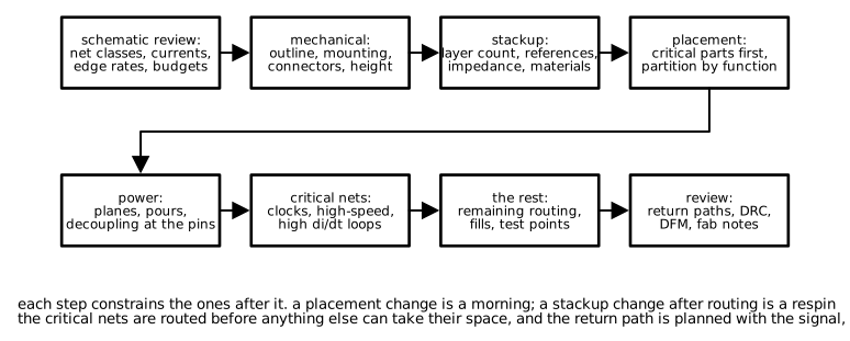 Figure 1. The layout sequence. Each step constrains the ones after it, so the decisions that are expensive to change are made first.
Layout is a sequence of decisions, and the order matters because each one removes freedom from the next. The sequence below is the one Hartley and Ritchey teach and the one experienced designers converge on.
- Schematic review before any copper. Classify every net: power and its current, ground, clocks and their edge rates, high-speed buses and their timing budgets, differential pairs and their impedance, sensitive analog inputs, high di/dt loops, cable-connected nets that need protection. Record the edge rate of every driver, not the clock rate; the edge sets the bandwidth. Assign net classes and design rules now, while the constraints are still in the designer's head rather than reconstructed from the board later.
- Mechanical constraints. Board outline, mounting holes, connector positions, height limits, heat sink and enclosure contact points, keep-outs, test point access, panelization. Connector positions are usually fixed by the product, and they fix the placement of everything that connects to them.
- Stackup. Layer count, which layers are planes, which planes are ground, dielectric thicknesses, copper weights, material. This sets the impedance of every trace, the inductance of every loop, and the crosstalk between every pair of neighbors. It is chosen before placement because the parts that need controlled impedance and the parts that need low-inductance power must know which layers give it to them.
- Placement, critical parts first. The switching converter and its hot loop, the clock and crystal, the RF section, the ADC and its front end, the BGA and its decoupling. Partition the board by function so that noisy and sensitive circuits are separated in space, on one unbroken ground plane. Then the connectors' support parts, then everything else.
- Power. Plane assignments, pours, the routing of every rail as a wide, short path with its return directly beneath it, and the decoupling capacitors at the pins with their vias in place. Power is routed before signals because a signal can detour and a power path cannot.
- Critical nets. Clocks, high-speed buses, differential pairs, length-matched groups, sensitive analog, the gate drive and current sense of every switcher. These are routed by hand, with the return path planned alongside, before the rest of the routing can take the space they need.
- Everything else. The remaining nets, ground fills where they serve a purpose, test points, silkscreen.
- Review. Every reference plane checked for gaps under traces, every high-speed via checked for a return via, DRC clean, DFM checked against the fabricator's capabilities, the fab drawing and stackup notes written.
The cost of a change grows along the list. A placement change is a morning. A stackup change after routing is a respin. A schematic change after fabrication is a rework station.
The physics that drives everything
The signal is the field
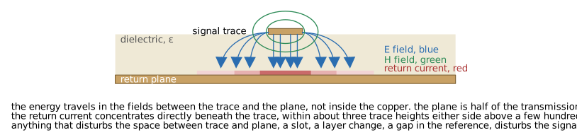 Figure 2. A microstrip in cross section. The energy of the signal is in the fields between the trace and the plane, and the return current in the plane concentrates beneath the trace.
A signal on a trace is not a current in a wire. It is an electromagnetic field in the dielectric between the trace and its return conductor, propagating at the speed of light in that dielectric, with a current on the trace and an equal and opposite current on the return as the boundary conditions of that field. The trace is one half of the transmission line and the plane is the other half. Every layout rule follows from three consequences of this picture.
The first is that the return current is not "in the ground". It is directly beneath the trace, and it spreads only about three trace heights either side. At DC and audio frequencies the return spreads across the plane to minimize resistance. Above a few hundred kilohertz the return follows the path of least inductance, which is the path that keeps the loop between signal and return smallest, and that path is directly under the trace. Bogatin's demonstration board, Hartley's return-current lectures, and every field solver show the same picture: the current density in the plane under a trace falls off as , with the distance from the trace centerline and the height above the plane, so 80 % of the return lies within three heights of the trace.
The second is that anything that disturbs the space between the trace and the plane disturbs the signal. A slot in the plane, a layer change to a different reference, a plane edge, a gap between two planes, a region of missing copper under a connector: each forces the return current to detour, and the detour is inductance in series with the signal, a discontinuity that reflects part of the edge, and a loop that radiates and couples.
The third is that the loop area between the signal and its return sets the inductance, and inductance sets almost every high-frequency problem: ground bounce, crosstalk, radiated emissions, susceptibility, and the impedance of the power distribution.
Loop inductance
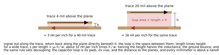 Figure 3. The loop between a trace and its return plane is the trace length times the height above the plane. Halving the height halves the inductance.
For a trace of width at height above a plane, with larger than , the loop inductance per length is approximately
A 10 mil trace 4 mil above the plane has about 13 nH per inch; the same trace 20 mil above the plane has about 64 nH per inch. The formula is approximate for narrow traces, where fringing fields add a logarithmic term, but the scaling is what matters: inductance is proportional to the height above the reference and inversely proportional to the width. The same rule applies to a power trace, a decoupling capacitor's loop, and a via. It is the reason thin dielectrics between signal layers and their planes are the single most valuable feature of a stackup.
The voltage developed across that inductance is . A 1 nH loop carrying an edge of 1 A per nanosecond drops 1 V. A 100 mA logic edge in 1 ns across 5 nH of ground path is 0.5 V of ground bounce. These are the numbers that make a 3.3 V logic family fail its noise margin.
Bandwidth of an edge
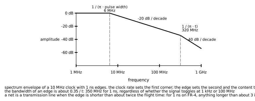 Figure 4. Spectrum envelope of a 10 MHz clock with 1 ns edges. The clock rate sets the first corner; the edge rate sets the content that matters for layout.
The bandwidth of a digital signal is set by its edge, not its clock. A trapezoidal edge of rise time has a spectrum that is flat up to , falls at 20 dB per decade to , and 40 dB per decade beyond. The useful bandwidth, the highest frequency with significant energy, is
A 1 ns edge has content to 350 to 500 MHz regardless of whether it toggles at 1 kHz or 100 MHz. A modern microcontroller GPIO has an edge of 1 to 2 ns; an FPGA output has 200 to 500 ps; a low-speed I2C line has 50 ns. The edge rate is what determines whether a net is a transmission line, how much it couples into its neighbors, and how much it radiates.
The rule for when a trace must be treated as a transmission line: when the round-trip delay of the trace is comparable to or longer than the edge. On FR-4 a signal travels about 6 inches per nanosecond, so the critical length is
Beyond that length an unterminated trace rings. For a 1 ns edge, 3 inches; for a 200 ps edge, 0.6 inches. Traces shorter than about one sixth of that behave as lumped elements and can be routed without regard to impedance. Between the two, termination is a judgment call informed by the receiver's tolerance to overshoot.
Transmission lines
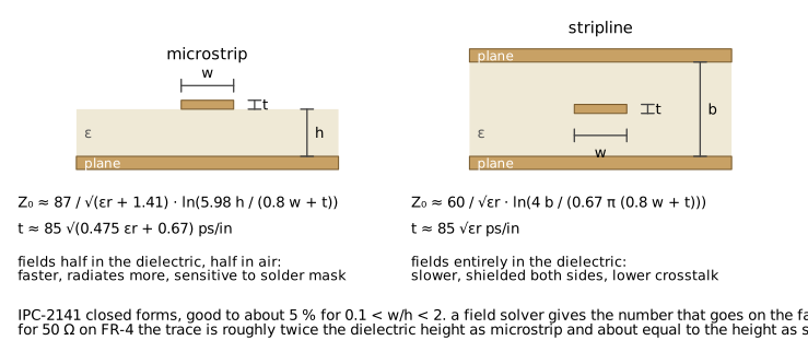 Figure 5. Microstrip and stripline in cross section with the closed-form impedance and delay expressions from IPC-2141.
A trace over a plane is a transmission line with a characteristic impedance set entirely by geometry and dielectric constant: , where and are the inductance and capacitance per length. Narrower trace or thicker dielectric raises ; wider trace or thinner dielectric lowers it. The closed forms in Figure 5 are from IPC-2141 and are good to about 5 % within their stated range; the number on the fabrication drawing comes from a field solver, either the fabricator's or a tool such as the Saturn PCB toolkit or Polar Si9000.
| Line type | Where the fields are | Delay on FR-4 | Notes |
|---|---|---|---|
| Microstrip | half in dielectric, half in air | about 140 to 150 ps/in | outer layers; solder mask lowers by 1 to 2 Ω; radiates and picks up more than stripline |
| Embedded microstrip | mostly in dielectric | about 160 ps/in | outer layer under a thick mask or a dielectric coat |
| Stripline | entirely in dielectric | about 170 to 180 ps/in | inner layers between two planes; shielded, lowest crosstalk, cannot be probed or reworked |
| Asymmetric stripline | entirely in dielectric | about 170 to 180 ps/in | inner layer closer to one plane; references the nearer plane mostly |
| Coplanar waveguide with ground | dielectric plus the gaps | between the two | RF; the side grounds must be stitched to the plane at a fraction of a wavelength |
For 50 Ω on FR-4, a microstrip is about twice as wide as its dielectric height; a stripline is about as wide as its height to the nearer plane. A 4 mil dielectric gives a 7 to 8 mil microstrip; a 3 mil dielectric gives about 5 mil. This is why thin dielectrics and narrow traces go together, and why a 62 mil two-layer board cannot have a 50 Ω trace of sensible width: it would need to be 110 mil wide.
Losses matter above about 1 GHz or over long runs. Conductor loss rises with through skin effect and with copper roughness; dielectric loss rises with through the loss tangent . Standard FR-4 has around 0.02; low-loss laminates have 0.002 to 0.005. At 5 Gb/s over 10 inches the difference is several decibels of eye closure.
Propagation delay and timing
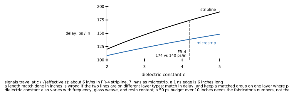 Figure 6. Propagation delay per inch for stripline and microstrip against dielectric constant. On FR-4 the two differ by about 20 %, which matters for any length match.
Signals travel at . For stripline and the delay on FR-4 is about 174 ps/in, or 6.9 mm per 50 ps. For microstrip, with half the field in air, and the delay is about 140 ps/in. The 20 % difference means a length match done in millimeters is wrong if the matched signals are on different layer types. Match in delay, and where a matched group must change layers, change them all the same way.
The timing budget for a source-synchronous bus, DDR memory for instance, is the sum of the clock-to-data skew the receiver tolerates, the driver's own skew, the crosstalk-induced jitter, and the routing mismatch. A typical DDR3 budget allows about 20 ps of routing mismatch within a byte lane, which is about 3 mm of stripline. Serpentine tuning to hit that number has its own rules: keep the serpentine segments at least 3 to 4 heights apart so the signal does not couple across them and arrive early, keep serpentines away from other signals, and put the tuning near the end of the route where the trace already has the mismatch. Match the whole path: package length, via depth, and connector pins count.
Dielectric constant is not one number. It varies with frequency, with the glass-to-resin ratio of the prepreg, and locally with the glass weave, so that a trace running over a glass bundle and its pair partner running over a resin window see different velocities. For a high-speed differential pair over a long run, the fiber-weave effect can add tens of picoseconds of skew. The mitigations are a spread-glass laminate, a route angled 10° to the weave, or a zig-zag route. For most boards below a few gigabits per second it does not matter; for a 10 Gb/s SerDes over 20 inches it does.
Stackup
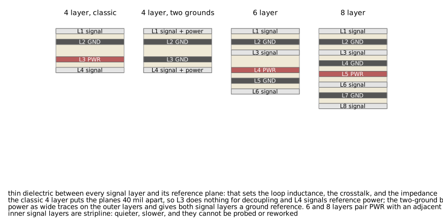 Figure 7. Four stackups. The rule in every one is a thin dielectric between each signal layer and a ground plane, and a thin dielectric between power and ground.
The stackup is the most consequential decision on the board and the one most often left to the fabricator's default. The stackup thickness cheat sheet has the tables; this section is about the reasoning.
What drives the decision
| Driver | What it demands of the stackup |
|---|---|
| Every signal layer needs a reference | A ground plane adjacent to each routing layer, on a thin dielectric. Two signal layers can share one plane between them. A signal layer with no adjacent plane is the most common stackup mistake. |
| Controlled impedance | A dielectric thickness that gives the target impedance at a manufacturable trace width. 50 Ω single-ended and 90 or 100 Ω differential on a 3 to 4 mil dielectric gives 4 to 6 mil traces, the practical minimum. |
| Power integrity | A power plane paired with a ground plane on the thinnest available dielectric; 2 to 4 mil gives 0.5 to 1 nF per square inch, which is the only capacitance that works above 200 MHz. |
| BGA breakout | Enough routing layers to escape every ring of balls. A 1.0 mm pitch BGA escapes two rows per layer with one trace between vias; a 0.8 mm pitch needs 4 mil traces or microvias; a 0.5 mm or 0.4 mm pitch needs HDI with via-in-pad microvias. Count the rings, divide by two, and that is the minimum number of routing layers for the breakout alone. |
| Current | Copper weight for the rails: 1 oz carries about 1 A per 20 mil of width for a 10 °C rise on an outer layer (IPC-2152); 2 oz halves the width. Heavy copper forces coarser trace and space everywhere on that layer. |
| RF sections | A low-loss, tightly toleranced dielectric under the RF traces, often a hybrid build with one Rogers or similar layer pair on top of an FR-4 core. Dielectric constant tolerance matters more than absolute value for a matched line. |
| Symmetry | A stackup symmetric about its center in copper weight and dielectric thickness, or the board warps in reflow. Balance copper coverage layer for layer. |
| Thickness | Connector and edge-finger standards, enclosure, and the drill aspect ratio: through-hole vias are limited to about 10:1 depth to diameter, so a 62 mil board needs a 6 mil drill or larger, and a 93 mil board needs 10 mil. |
| Cost | Standard builds, standard materials, standard thicknesses. Every non-standard item is a cost step. HDI with microvias is a large step. Blind and buried vias are a large step. |
The four-layer question
The classic four-layer build, signal / ground / power / signal, puts the two planes about 40 mil apart on a 62 mil board. That spacing gives almost no plane capacitance, so the power plane contributes nothing to decoupling above a few megahertz, and the bottom signal layer references the power plane, which means every bottom-layer return current has to find a capacitor to get to ground. Hartley's recommendation, which Ritchey and Peterson share, is signal / ground / ground / signal for a four-layer board carrying anything fast: both signal layers get a ground reference, the two ground planes are stitched together by vias everywhere, and power is routed as wide traces and small pours on the outer layers, decoupled locally. The 40 mil of core between the two ground planes then carries nothing that matters.
On a six-layer board the classic choice is signal / ground / signal / power / ground / signal, which gives every signal layer a ground reference except L3, which references L2 from above, and puts the power plane against a ground plane. An eight-layer build has enough planes to pair every signal layer with a ground and still keep a power-ground pair.
Materials
Standard FR-4 (Dk about 4.2 to 4.6 at 1 GHz, tan δ about 0.02) is adequate to about 3 Gb/s or 2 GHz. Mid-loss laminates (Isola 370HR, FR408HR, Panasonic Megtron 4) extend that to 10 Gb/s. Low-loss (Megtron 6, Rogers 4350B, Tachyon) are for 25 Gb/s and above, or for RF where the phase must be stable. Rogers 4003C and 4350B are the usual choice for an RF layer pair because they process like FR-4. PTFE laminates do not, and cost accordingly. Specify the material by name and glass style on the fab drawing, not "FR-4", when impedance or loss is controlled; "FR-4" is a flammability rating, not a material.
Placement
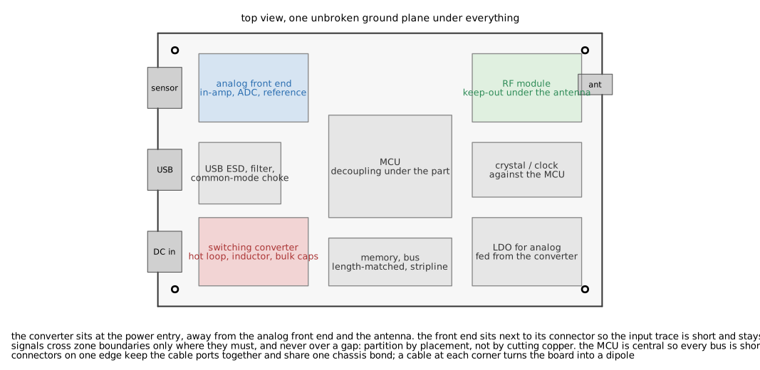 Figure 8. A placement partitioned by function on one unbroken ground plane. Noisy circuits sit at one end near their connectors, sensitive circuits at the other, the processor in the middle.
Placement decides most of the electrical outcome before a trace is drawn. The principles:
- Partition by function, on one plane. Group the switching converter, the digital core, the analog front end, and the RF section into their own regions. Separation in space is what gives isolation; the field of a switching loop falls off with distance, and a sensitive trace that never enters the noisy region never picks it up. The plane under all of it stays whole. Cutting the plane between regions is the mistake covered in the next section.
- Critical parts first, at their connectors. The converter at the power entry, so its input filter is short and its output does not have to cross the board. The analog front end at its sensor connector, so the high-impedance input trace is a few millimeters. The RF module at the antenna. The ESD and filtering of every cable port at that port. Then the processor in the middle, where every bus is short, and everything else around it.
- Cable ports on one edge. Every cable is an antenna driven by the common-mode voltage between its port and the rest of the board. Ports on one edge share one chassis bond and a short path between them; a port on each corner puts the board's noise across a dipole whose length is the board.
- Orient parts for the flow of the signal. An ADC with its analog pins facing the front end and its digital pins facing the processor needs no crossing. A converter with its input capacitor, switch, and diode in a triangle has a smaller hot loop than one with them in a row.
- Decoupling before anything else near a part. The decoupling capacitors of a BGA go in first, on the bottom side directly under the balls or on the top within a few millimeters of the pins, with their vias. What space remains is for the rest.
- Thermal. Hot parts away from temperature-sensitive ones, near the airflow or the heat sink, with copper pours and thermal vias sized for the dissipation. A voltage reference next to a regulator drifts; a crystal next to a power FET loses frequency.
- Mechanical and assembly. Tall parts away from the enclosure walls, connectors accessible, keep-outs around mounting holes, polarized parts oriented consistently, fiducials in place, test points reachable, no parts in the panel rails. Check the assembly house's rules for minimum part-to-part spacing and edge clearance before placing anything.
Grounding and the return path
Grounding is the subject with the most folklore. The ground planes note covers it in full; the essentials and the myths are collected here.
One unbroken plane
The ground plane's job is to be the return conductor of every signal and every power rail on the board, directly beneath each, with no interruption. A whole plane has an impedance of milliohms at DC and a spreading inductance of tens of picohenries between any two points, which is as close to a zero-impedance reference as a board can have. Every trace over it has its return under it. Every capacitor to it has a short loop. Every region of the board is at the same potential to within the noise of the return currents that cross it, and the way to keep that noise away from a sensitive circuit is to keep the noisy currents from crossing under it, which is a matter of placement.
The split-ground myth
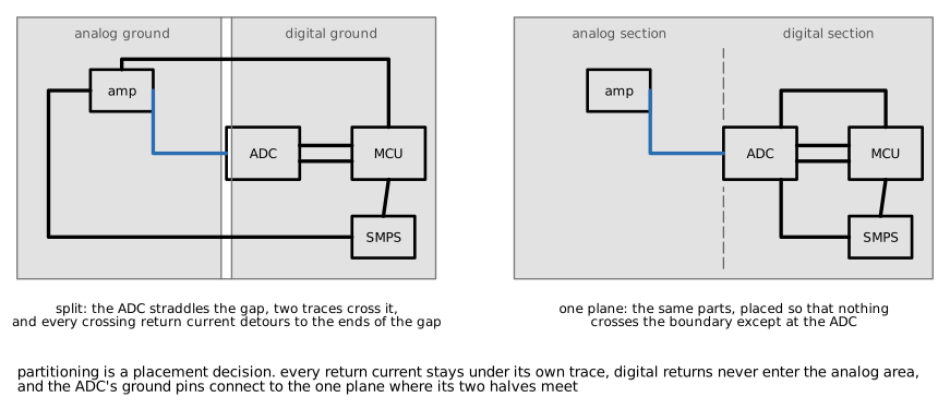 Figure 9. The same circuit on a split plane and on one plane. On the split, the ADC bridges the gap and every signal that crosses becomes a loop; on one plane the partition is by placement.
The myth: analog and digital grounds must be separate copper regions, joined at one point, to keep digital noise out of analog. The physics: a signal crossing the split has no return path under it, so its return detours around the end of the split, the loop opens to the length of the detour, and the signal radiates, picks up, and reflects at the crossing. Every trace that crosses the split does this, and something always crosses it: the ADC's own data lines, the supply, the reference. The voltage between the two regions is set by the current forced across the single joining point, which is exactly the common-impedance coupling the split was meant to prevent. Hartley's phrasing: a split creates a slot antenna, and the traces crossing it are the feed.
The alternative that achieves what the split was meant to achieve is partition by placement. Put the analog circuits in one region and the digital circuits in another, on one plane, and let no digital trace enter the analog region. The digital return currents then stay under the digital traces, in the digital region, and the analog region's plane carries only analog returns. The ADC sits on the boundary with its analog pins toward the analog region and its digital pins toward the digital region. This is what the datasheets of every precision ADC vendor now recommend when read carefully; the split-ground drawings in older application notes date from two-layer boards where there was no plane to keep whole.
The one legitimate split is galvanic isolation: two grounds that must be at different potentials, with every crossing made by an isolator, a transformer, or an optocoupler, and nothing else in common. That is not "separating analog and digital"; it is two separate boards that happen to share a laminate.
Where the return current goes when the reference changes
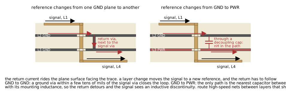 Figure 10. A signal changing layers. The return current has to change planes too. Between two ground planes a nearby via closes the loop; between ground and power the only path is a capacitor.
A signal via moves the signal from one layer to another, and the return current has to move from one plane's surface to another's. Between two ground planes, the return needs a ground via within a few tens of mils of the signal via; without one it spreads out to find the nearest stitching via, and the loop it opens is inductance and a radiating slot. Between a ground plane and a power plane the only path is the nearest capacitor between them, with its mounting inductance in series, and the return detours to it. The rules:
- Route high-speed nets on layers that share a ground reference, or on the two sides of one ground plane.
- Put a ground via next to every signal via on a critical net, closer than a tenth of the wavelength at the knee frequency. For a 1 ns edge that is under about 100 mil; place it as close as the annular rings allow.
- Where a reference change to power is unavoidable, place a 10 to 100 nF capacitor between the two planes adjacent to the via.
- Stitch ground planes together with a via grid at about a tenth of a wavelength at the highest frequency of concern: 100 to 200 mil spacing for a board with 1 ns edges, tighter near high-speed nets and at plane edges.
Two-layer boards and chassis
A two-layer board has no plane worth the name unless one side is left almost entirely as ground and the other carries the signals, with every crossing on the ground side kept short and every trace on the signal side kept over uninterrupted ground. A ground pour full of islands and long slots is worse than a few well-placed return traces, because it looks like a plane and is not. For a two-layer board with a switching converter, the converter's loop must be closed on one layer.
Chassis ground is a separate net that touches the board's ground at the cable ports, in one place per port and as short as possible. The connector shell, the ESD diodes, and the shield of every cable go to chassis; the board's ground bonds to chassis right there, through a direct connection or a high-voltage capacitor if the product requires isolation at low frequency. A bond anywhere else puts the board's noise current through the chassis and out the cable. The noise note covers shield termination.
Routing critical nets
Terminations and reflections
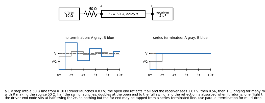 Figure 11. A 1 V step from a 10 Ω driver into a 50 Ω line with an open end, without and with a series termination. The unterminated line rings for many round trips; the terminated line settles in one flight time.
At every change of impedance a fraction of the incident wave reflects. An open end reflects everything with , so the voltage there doubles. A low-impedance driver reflects with near , so the reflection comes back inverted. Between them the wave bounces until the mismatches absorb it. The receiver sees overshoot, undershoot, and a stair-step edge that can cross the threshold more than once.
| Termination | Where | Value | Cost | Use |
|---|---|---|---|---|
| Series | at the driver | one resistor, no DC current | point to point, one receiver at the far end; the driver end sits at half swing for one round trip, so no tap in the middle | |
| Parallel to ground | at the receiver | DC current, half the swing for a weak driver | fast edges into a single load, when the driver can source the current | |
| Thevenin | at the receiver | two resistors, parallel value , ratio sets the idle level | DC current | buses that must idle at a defined level |
| AC (RC) | at the receiver | , so that is about 3 bit times | no DC current, adds a load | clocks and periodic signals |
| Differential | at the receiver | between the pair, or two to a center tap | small | every differential standard; the receiver often has it on chip |
| On-die | inside the receiver | configured by the IC | none | DDR, PCIe, most SerDes; set it in the IC's registers and match the board to it |
A series termination is the default for a point-to-point logic signal longer than the critical length. A parallel termination is for multi-drop buses, where the series scheme's half-swing plateau would be seen by the intermediate taps. Fly-by topology with the termination past the last load, as in DDR3 and later, is a parallel termination with the stub lengths kept below the critical length.
Stubs are the hidden reflection. A branch off a line, a via that continues through the board past the layer where the signal leaves it, a test point on a long trace: each is an unterminated line whose reflection arrives at a delay equal to twice the stub length. For a 200 ps edge, a stub over about 50 mil matters. Back-drilling removes the unused part of a through via for this reason on boards above a few gigabits per second; blind or micro vias avoid creating it.
Differential pairs
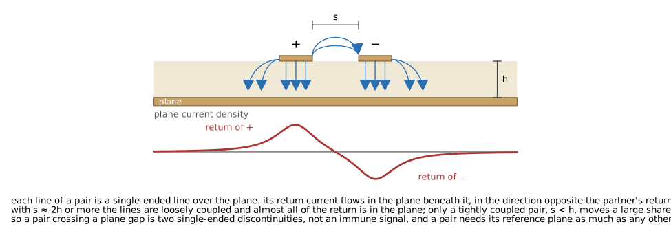 Figure 12. A differential pair over a plane. Each line's return current is in the plane beneath it, not in the partner line, unless the pair is much closer to each other than to the plane.
A differential pair is two single-ended transmission lines driven with opposite signals. The receiver responds to the difference, which rejects whatever is common to both: ground offset between driver and receiver, common-mode noise picked up along the way, and the reference shift when the pair crosses something. The differential impedance is the impedance seen between the two lines, , where the odd-mode impedance is somewhat less than the single-ended because of the coupling between the lines. For loosely coupled pairs, spacing of two or more heights, and the lines can be treated independently.
Where the return current goes is the point most often misunderstood. Each line's return is in the plane directly beneath it, in the opposite direction to the partner's return, and only a fraction is carried by the partner, a fraction that rises as the pair is brought closer together than the height above the plane. A typical 100 Ω pair with spacing equal to the trace width and a 4 mil dielectric has most of its return in the plane. So a pair crossing a plane gap is two single-ended discontinuities. The common-mode rejection of the receiver removes the shared part of the disturbance, but the mode conversion at the gap, the radiation from the two loops, and the impedance discontinuity are not removed. Differential pairs need their reference plane like any other trace; they merely fail more gracefully without it.
The practical rules:
- Keep the pair the same length to within the skew budget, which is a fraction of the bit time: for 5 Gb/s, about 5 to 10 ps, or 1 to 2 mm. Match at the point where the mismatch occurs, not at the far end.
- Keep the spacing constant along the route, since the differential impedance depends on it; open the pair around obstacles only where unavoidable and for as short a distance as possible.
- Route the pair on one layer with the fewest possible vias, and where vias are needed, place them as a pair with ground vias beside them.
- Keep other signals at least three heights away, and other pairs at least three heights away from each other. Tight coupling within a pair does not reduce crosstalk from a neighbor as much as distance does.
- AC-coupling capacitors, ESD diodes, and connector pads are discontinuities; keep them small (0402 or smaller), symmetric between the two lines, and adjacent to each other, and cut the plane under a large pad to restore the impedance if the tool models it.
Crosstalk
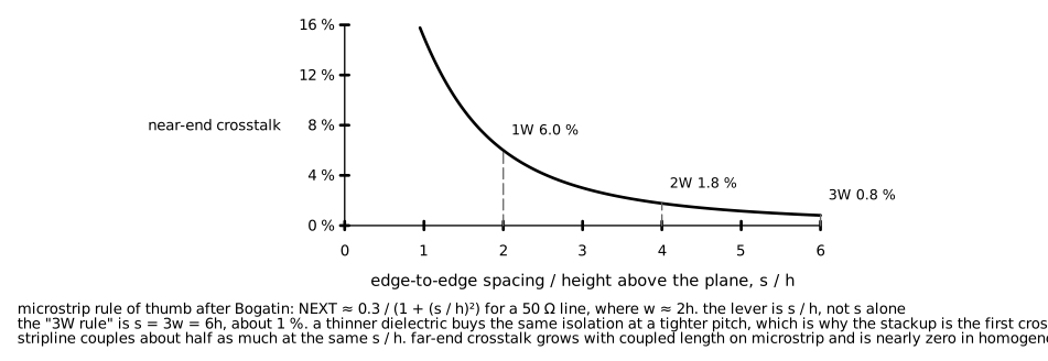 Figure 13. Near-end crosstalk against the ratio of spacing to dielectric height for a microstrip. The lever is the ratio, not the spacing alone.
Two traces near each other share fields. The aggressor's edge induces a current in the victim through mutual capacitance and a voltage through mutual inductance; the two add at the near end (the end nearer the aggressor's driver) and subtract at the far end. Near-end crosstalk is a fixed fraction of the aggressor's swing that lasts for twice the coupled length's delay; far-end crosstalk is a pulse that grows with coupled length and with edge rate, and on stripline is nearly zero because the capacitive and inductive parts cancel in a homogeneous dielectric.
The coupling depends on the ratio of spacing to height above the plane, because the height sets how far the fields spread. Bogatin's rule of thumb for a 50 Ω microstrip: near-end crosstalk is about 6 % at a spacing equal to the trace width, under 2 % at twice the width, and about 1 % at three times. The 3W rule that appears in every guideline is this last number. It is a rule for a trace width about twice the height; it is neither necessary on a thin dielectric nor sufficient on a thick one. A board with a 3 mil dielectric can route at a tighter pitch for the same isolation than one with an 8 mil dielectric, and that is the crosstalk argument for thin dielectrics, in addition to the inductance argument.
Guard traces, a grounded trace run between two signals, are of limited value: they work only if stitched to the plane at intervals much shorter than a wavelength, and at that point the same space given to spacing does as well. On a board with a solid adjacent plane, distance and a thin dielectric are the tools. A guard ring around a high-impedance analog node is a different device, for leakage rather than crosstalk, and does work.
Crosstalk is also a timing problem: an aggressor edge arriving during a victim edge shifts the victim's crossing point, which is jitter. For a matched bus the crosstalk budget is part of the timing budget.
Power integrity
The impedance target
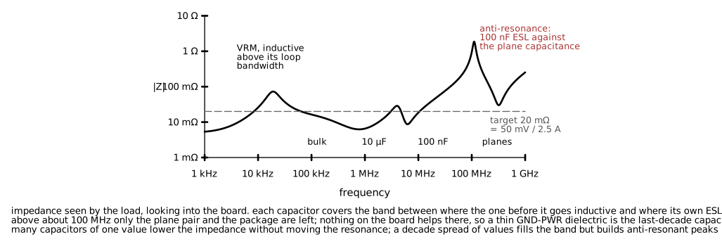 Figure 14. Impedance of a power distribution network from the regulator to the die. Each capacitor covers one band; above about 100 MHz only the plane pair and the package are left.
A power rail must hold its voltage within a tolerance while the load draws a current that changes in nanoseconds. The rail looks to the load like an impedance, and the requirement is
A 1 V core rail allowed 50 mV of ripple under a 2.5 A step must present under 20 mΩ from DC to the highest frequency at which the load's current changes, which is the bandwidth of the load's edges, hundreds of megahertz for a digital core. No single component covers that range. The regulator holds the impedance low up to its loop bandwidth, tens of kilohertz to a megahertz. Bulk capacitors, tens to hundreds of microfarads, cover to a few hundred kilohertz before their inductance takes over. Ceramic capacitors of 1 to 10 µF cover to a few megahertz; 100 nF parts to a few tens of megahertz; and above that the only capacitance with low enough inductance is the plane pair itself, then the package and the die.
Each capacitor is a series RLC: below its resonance it is a capacitor, above it an inductor. The inductance is almost entirely the mounting, not the part. Where one capacitor's inductive region meets the next's capacitive region there is a parallel resonance, an anti-resonant peak at which the impedance rises above both. The design of a decoupling network is the management of these peaks: enough capacitors of each value that the peaks stay under the target, and enough resistance (ESR) that they are damped.
Two conclusions follow, both counter to habit. First, many capacitors of the same value in parallel lower the impedance without moving the resonance, and adding a decade-spaced set of values (100 nF, 10 nF, 1 nF) creates anti-resonant peaks between them that may be higher than the impedance would have been with one value; it is a technique that needs simulation, not a default. Second, the capacitor's value matters less than its loop: a 100 nF part with 3 nH of mounting inductance is inductive above 9 MHz, and no choice of value changes that.
Mounting inductance
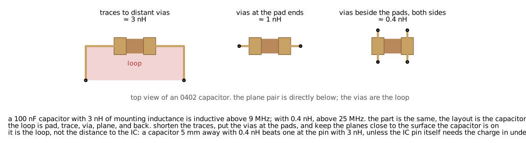 Figure 15. Three ways to mount the same 0402 capacitor. The loop through the pads, the traces, and the vias to the planes is the inductance, and it varies by nearly an order of magnitude with the layout.
The loop of a decoupling capacitor is the pad, the trace to the via, the via down to the plane, the plane pair, and back up the other via. Its inductance is proportional to the area of that loop. A capacitor with its vias at the ends of long traces has 2 to 3 nH; with the vias at the pad ends, about 1 nH; with vias on both sides of each pad, or via-in-pad, 0.3 to 0.5 nH. The distance to the plane pair adds to it: a plane pair 4 mil below the surface gives a much smaller loop than one 30 mil below. This is a stackup decision, and it is the reason the ground plane goes on layer 2 and the power-ground pair is placed close to the layer that carries the decoupling.
The question of how close the capacitor must be to the IC is answered by the same loop argument. Below a few hundred megahertz the capacitor's own loop inductance dominates, and a capacitor 5 mm away with 0.4 nH is better than one at the pin with 3 nH. Above that, the spreading inductance of the plane between the capacitor and the pin, and the pin's own package inductance, dominate, and only the plane pair and the on-package capacitance help. Put the capacitors close because it costs nothing, but put the vias right because it is what matters.
Plane capacitance and cavity resonance
A power plane and a ground plane on a thin dielectric are a capacitor of : about 0.9 nF per square inch at 2 mil, 0.45 nF at 4 mil, 0.2 nF at 10 mil. That is small, but it comes with an inductance of picohenries, and so it is the only capacitance that works above a few hundred megahertz. A pair of planes is also a resonant cavity, with its first mode at : for a 4 inch plane pair on FR-4, about 700 MHz. At the cavity resonances the plane impedance peaks and the edges of the board radiate. Close spacing raises the losses that damp the resonance, and stitching vias with capacitors between the planes at the board edges damp it further. The 20H rule, pulling the power plane back from the edge by twenty times the dielectric thickness, addresses the same radiation; on a thin dielectric with edge stitching it is unnecessary, and on a thick one it is insufficient.
High di/dt and high dV/dt circuits
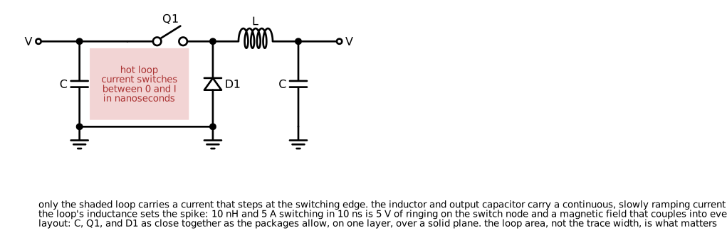 Figure 16. The loops of a buck converter. The hot loop is the difference of the on-state and off-state loops; the gate drive loop is the third.
A switching converter has three loops that matter and two noisy nodes. The on-state loop runs from the input capacitor through the switch and inductor into the output capacitor; the off-state loop runs from the inductor through the freewheeling element into the output capacitor. Their difference, the input capacitor, the switch, and the diode or synchronous switch, is the hot loop, the only path whose current steps at the switching edge. The gate drive loop, from the driver through the gate resistor into the gate and back through the source, carries amperes for tens of nanoseconds. The switch node is the high dV/dt node; the hot loop is the high di/dt loop. The noise note and the SMPS note cover the circuits; the layout rules are:
- Place the input capacitor, the switch, and the diode or low-side switch as close together as the packages allow, on one layer, with the loop closed on that layer, over an unbroken ground plane. The loop area, not the trace width, sets the inductance and the ringing. 10 nH of loop with 5 A switching in 10 ns is 5 V of overshoot on the switch node.
- Keep the switch node copper as small as the current allows. It is a capacitor plate driven at tens of volts per nanosecond; every square millimeter couples into whatever is under or beside it. Do not put a plane cut under it; put a ground plane under it and accept the small capacitance to ground, which is far less harmful than the radiation from an unshielded node.
- Place the gate driver against the switch, with the gate resistor and the bootstrap capacitor at the pins, and route the gate and its return as a pair.
- Route the current-sense lines as a differential pair from the sense resistor's pads, Kelvin-connected, away from the switch node and the inductor.
- Keep the feedback divider and the compensation network close to the controller, away from the inductor and the switch node, and reference them to the controller's ground pin.
- Give the inductor a keep-out for sensitive traces on the layers beneath it, or use a shielded inductor and still keep the front end away from it.
The same rules apply, scaled down, to every digital output: the current that charges the load capacitance flows from the decoupling capacitor through the driver and the trace into the load and back through the plane, and that loop is a small hot loop. A 3.3 V driver charging 20 pF in 1 ns draws 66 mA for that nanosecond. A bus of thirty-two such drivers switching together draws 2 A, and the ground bounce across the package and via inductance is what the term simultaneous switching noise refers to.
EMC
Emissions and susceptibility are decided by the same fields that decide signal integrity. A board that keeps every return under its signal, every loop small, and every plane whole radiates little from the board itself; what remains is the cables.
Cables are the antennas
A board is a poor antenna: its longest dimension is a small fraction of a wavelength below a few hundred megahertz. A cable a meter long is a good antenna from 30 MHz up. The current that drives it is the common-mode current, the current that flows out on all the conductors of the cable together and returns through the environment. Its source is the voltage between the point where the cable attaches and the board's reference, which is the ground bounce, the return current across a slot, the power rail noise, whatever the board puts across that path. A few microamps of common-mode current on a one-meter cable is enough to fail a Class B radiated emissions limit at 100 MHz.
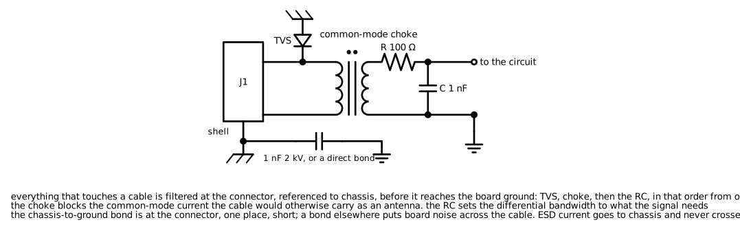 Figure 17. Filtering at a cable port. The TVS, the common-mode choke, and the RC sit at the connector, referenced to chassis, before the signal reaches the board ground.
The defenses are at the port. A common-mode choke on the cable's conductors raises the impedance the common-mode current sees without affecting the signal. A filter on each line sets the bandwidth to what the signal needs. The connector shell and the cable shield bond to chassis at the connector, and the board's ground bonds to chassis at the same place, once, so that no board current flows through the chassis path. ESD protection sits at the connector with its return to chassis, so that the ESD current never crosses the board. A ground pour under the connector area, stitched to chassis, is the low-impedance reference for all of it. Every cable port gets this treatment; the one that does not is the one that fails.
Board-level practices
- Stitch every ground plane to every other with a via grid, and stitch the board edges at a spacing under a tenth of the wavelength at the knee frequency.
- Keep clocks and switch nodes away from the board edges and away from connectors.
- Do not route any signal over a plane gap or off the edge of a plane, including under connectors, near mounting holes, and around cutouts.
- Terminate every clock and every fast edge. An unterminated edge rings at the resonance of the trace, and that ringing has a spectrum that peaks exactly where the emissions test looks.
- Slow the edges where the design allows. A series resistor at every non-critical driver, 22 to 33 Ω, costs nothing and removes the top decade of the spectrum.
- Spread-spectrum clocking lowers the peak of each harmonic by spreading it; it helps the measurement more than it helps the neighbor.
- Shielding cans work when the can is bonded to the plane around its entire perimeter at a spacing under a tenth of a wavelength; a can with a few tabs is a resonator.
- Mounting holes that bond the board to a metal chassis at several points give the board a low-impedance reference to the chassis and lower the common-mode drive to every cable. Use them.
Fabrication and assembly
Every electrical rule has to survive contact with the fabricator's process. The limits that matter:
| Parameter | Standard capability | Advanced | Note |
|---|---|---|---|
| Trace and space, 1 oz outer | 5 / 5 mil | 3 / 3 mil | 4 / 4 mil is the common cost floor; each step below is a cost step |
| Trace and space, 2 oz | 8 / 8 mil | 6 / 6 mil | heavy copper needs wider space to etch |
| Drill, mechanical | 8 mil finished | 6 mil | smaller drills need thinner boards (aspect ratio) and cost more |
| Microvia | 4 mil laser, one layer deep | stacked or staggered | HDI build; via-in-pad for fine-pitch BGA |
| Annular ring | 5 mil | 3 mil | set by drill registration; pads smaller than drill plus 10 mil fail |
| Aspect ratio | 8:1 | 12:1 | board thickness over drill diameter for a through via |
| Solder mask dam | 4 mil | 3 mil | between pads of fine-pitch parts; below this the mask is removed |
| Copper to edge | 10 mil | 8 mil | more at V-score lines: 20 mil |
| Impedance tolerance | ±10 % | ±5 % | ±5 % requires controlled dielectric and a coupon |
| Finish | HASL, ENIG, immersion silver, OSP | ENEPIG | ENIG for fine pitch and flat pads; nickel in ENIG adds loss above a few gigahertz |
Design rules for fabrication and assembly:
- Ask the fabricator for their stackup library and capability sheet before choosing trace widths, and put the chosen stackup, the materials by name, the impedance requirements with the layer and trace width for each, the copper weights, and the finish on the fabrication drawing.
- Request an impedance coupon and a report when impedance is controlled.
- Use thermal reliefs on plated through-hole pads and on the pads of parts hand-soldered; use direct connections on SMD pads to planes only where the assembly process supports it, since a pad tied to a plane sinks heat and produces tombstoning on small parts if the other pad is not.
- Tent vias that are under parts or near fine-pitch pads; leave test vias open. Fill and cap vias in pads.
- Keep the copper balanced across the board and across the stackup, or the panel warps; add copper thieving where needed.
- Provide fiducials, at least three global and local pairs at fine-pitch parts. Keep the panel rails clear.
- Check the paste layer: pad size and paste aperture for every footprint, reduced apertures on large thermal pads, and no paste on test points.
- Check every footprint against the manufacturer's recommended land pattern, and every polarized part's pin 1 against the silkscreen and the assembly drawing.
Common mistakes
The mistakes below account for most of what a review of a first-pass layout finds.
- A signal layer with no adjacent reference plane. Traces on a layer whose nearest plane is 40 mil away are 40 mil high loops. Fix the stackup.
- A plane split under a signal, or a signal routed over a plane gap. Includes the antipad field under a connector, the moat around a mounting hole, the cutout for a heat sink, and the gap between a power pour and the ground around it under a bottom-layer trace.
- A separate analog ground. See above. Partition by placement.
- Decoupling capacitors with long traces to their vias, or on the wrong side of the board from the plane pair, or missing entirely from the pins that need them most.
- A converter hot loop that spans two layers or a long path. The input capacitor on the far side of the inductor, or on the bottom of the board from the switch.
- A switch node with a large pour "for thermal reasons". The heat goes into the ground plane through the diode's or the low-side switch's thermal pad, not the switch node.
- A high-speed via with no return via. Or a via that changes the reference from ground to power with no capacitor nearby.
- A pair length-matched in millimeters across a layer change, or a matched bus with serpentines coupled to themselves.
- An unterminated clock, or a clock routed on an outer layer past a connector.
- A crystal with its load capacitors far from the pins, or the crystal traces crossing other signals. The crystal is the most sensitive high-impedance node on most boards.
- Analog input traces routed through the digital region, or beside a clock, or under the inductor.
- A cable port with its ESD diodes returning to board ground through a long path, or its filter on the far side of the board from the connector.
- Ground pours full of islands and slivers. Every island is a resonator, every sliver a stub; a pour that is not stitched to the plane at short intervals is worse than no pour.
- Chassis bonded to ground at several points across the board. The board's return currents then flow through the chassis.
- Right-angle bends. These do not matter electrically below several gigahertz; the myth persists because acid traps were a fabrication problem in the 1970s. The width change at a corner is a fraction of a picofarad. Mitered or curved corners are for the RF layers and for length-matched pairs where the outer and inner traces of a bend would otherwise differ in length.
- Vias treated as free. Each via is 0.5 to 1 nH, 0.3 to 0.5 pF, and a stub if it continues past the exit layer. On a slow net none of that matters; on a fast one every via is a discontinuity.
- Thermal management left to the end. A part that needs a copper area and thermal vias needs the space reserved at placement.
- DFM checked after routing. The footprints, the fabricator's capabilities, and the assembly house's rules belong in the design rules before the first trace.
Review checklist
Before release, check every item against the board, not against memory.
- Every signal layer has a ground plane adjacent to it, and no trace crosses a gap in that plane.
- Every high-speed via has a ground via within 100 mil, and no high-speed net changes its reference to a power plane.
- Every decoupling capacitor has its vias at the pad ends or beside the pads, and its loop is on the surface closest to the plane pair.
- Every converter's hot loop is on one layer, as small as the packages allow, over an unbroken plane, with the switch node copper minimal and the gate loop closed at the switch.
- Every clock, every bus, and every pair is terminated as its standard requires, length-matched in delay, and routed away from edges and connectors.
- Every cable port has its ESD, filtering, and chassis bond at the connector, and the connector's ground pour is stitched to chassis.
- Every sensitive analog trace stays in its region, over its own quiet plane area, away from clocks, switch nodes, and inductors.
- Every ground plane is stitched to every other with a via grid, including at the board edges.
- The stackup on the fab drawing matches the one the impedances were calculated for, by material name, thickness, and copper weight, with an impedance coupon requested.
- DRC is clean against the fabricator's rules, footprints verified, paste and mask layers checked, fiducials and test points present, copper balanced.
Rules of thumb
| Quantity | Rule | Source |
|---|---|---|
| Edge bandwidth | Bogatin | |
| Critical length | half the edge's flight distance: 3 in per ns of edge on FR-4 | Bogatin, Johnson |
| Velocity on FR-4 | 6 in/ns stripline, 7 in/ns microstrip; 170 and 140 ps/in | IPC-2141 |
| Return current spread | 80 % within three heights of the trace centerline | Bogatin, Hartley |
| Loop inductance, wide trace | , 32 nH/in times | Bogatin |
| Via inductance | about 1 nH per 40 mil of length; 0.5 to 1 nH for a through via | Johnson |
| Decoupling mounting inductance | 0.3 to 3 nH depending on via placement | Bogatin, Ritchey |
| Plane capacitance | about 0.9 nF per square inch per 2 mil of FR-4 | derived |
| Near-end crosstalk, microstrip | 6 % at 1W, 2 % at 2W, 1 % at 3W for | Bogatin |
| Stitching via spacing | under a tenth of a wavelength at the knee frequency; 100 to 200 mil for 1 ns edges | Ott, Hartley |
| 50 Ω microstrip width | about 2 times the dielectric height | IPC-2141 |
| 50 Ω stripline width | about equal to the height to the nearer plane | IPC-2141 |
| Current capacity, 1 oz outer | about 1 A per 20 mil for 10 °C rise | IPC-2152 |
| Common-mode current to fail Class B | a few microamps on a 1 m cable at 100 MHz | Ott |
References
- Eric Bogatin, Signal and Power Integrity, Simplified, 3rd edition. The physics of return current, transmission lines, crosstalk, and the PDN, with the rules of thumb used above.
- Eric Bogatin, Bogatin's Practical Guide to Transmission Line Design and Characterization for Signal Integrity Applications.
- Rick Hartley, "How to Achieve Proper Grounding" and "PCB Layer Stackup", AltiumLive 2019 and 2020 talks, and his Bogatin/Hartley discussions on return currents; the source of the two-ground four-layer stackup and the argument against splits.
- Lee Ritchey, Right the First Time: A Practical Handbook on High Speed PCB and System Design, Volumes 1 and 2. Stackup, PDN, and the design process.
- Henry Ott, Electromagnetic Compatibility Engineering. Grounding, cables as antennas, common-mode current, shielding, and the numbers for emissions.
- Howard Johnson and Martin Graham, High-Speed Digital Design: A Handbook of Black Magic and High-Speed Signal Propagation: Advanced Black Magic.
- Zachariah Peterson, Altium Academy and the Altium blog: stackup design, differential pair return paths, PDN impedance, and the fiber-weave effect.
- Dan Beeker, NXP, "Field-based PCB design" and the "Fields are the signal" lecture series.
- Istvan Novak, Power Distribution Network Design Methodologies, and his papers on decoupling capacitor selection and anti-resonance.
- IPC-2141A, Design Guide for High-Speed Controlled Impedance Circuit Boards. IPC-2152, Standard for Determining Current Carrying Capacity in Printed Board Design. IPC-2221B, Generic Standard on Printed Board Design. IPC-6012, Qualification and Performance Specification for Rigid Printed Boards.
- Texas Instruments, SLVA043, "Power Supply Layout Guidelines", and Analog Devices AN-1149, "Layout Techniques for Switching Power Supplies", for the converter loops.
- Saturn PCB Design Toolkit and Polar Si9000 for impedance, delay, and current-capacity calculations.