Thermal Design
noteGetting heat out of a part on a board: the junction-to-ambient chain and its electrical analogy, why the datasheet θja is not a design number, the two parallel paths out of a surface-mount package, PCB copper as the heatsink, thermal vias, heatsink sizing with and without airflow, transient thermal impedance for pulses, measuring junction temperature, a design procedure, and a worked example.
related tools: junction temperature, linear regulator thermal, thermal resistance chain, trace width (ipc-2221), via current / resistance / inductance
Scope: steady-state and transient thermal design for components on printed circuit boards, from a few hundred milliwatts in a small package to tens of watts on a heatsink. The note covers the thermal resistance model, the datasheet parameters and their test conditions, the board as a heatsink, external heatsinks, pulse ratings, and verification. Liquid cooling, heat pipes, and system-level enclosure thermal design are mentioned only where they set a boundary condition.
Common errors
- Using θja from the datasheet as a design number. It is measured on a JEDEC test board with a defined copper area in still air, and describes that board. On a small board with little copper the real value can be double; on a large board with a pour it can be half.
- Forgetting that most SMD heat leaves through the pad. For a package with an exposed pad, 80 to 90 % of the heat goes into the board. The board layout, not the package, sets the junction temperature.
- Sizing copper by the pad alone. The pad conducts heat into the copper around it; the pour area and the vias to the other side are what dissipate it.
- Adding thermal vias without a pour on the far side. The vias conduct heat to nothing.
- Treating a heatsink's θsa as a constant. It depends on airflow, orientation, mounting pressure, and the temperature rise itself.
- Ignoring the interface. A dry, rough contact between a package and a heatsink can add more resistance than the heatsink itself.
- Sizing for average power when the load is pulsed. A pulse shorter than the thermal time constant sees a much lower impedance; sizing for the average is wasteful. A pulse longer than it sees nearly the steady-state value; sizing for the average is dangerous.
- Stopping at a calculation. The thermal model has a factor-of-two uncertainty. The design is verified with a measurement.
The thermal resistance model
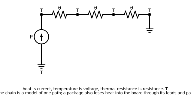 Figure 1. The thermal chain from junction to ambient as an electrical circuit. Heat flow is current, temperature is voltage, thermal resistance is resistance.
Heat flow in steady state obeys the same equation as current flow: a temperature difference drives a heat flow through a thermal resistance. With P in watts and θ in °C/W:
The terms:
| Symbol | Path | Set by | Typical values |
|---|---|---|---|
| θjc | Junction to the case surface (top, or the exposed pad, and the datasheet says which) | Die attach, lead frame, mold compound | 0.3 to 5 °C/W for power packages, 20 to 60 °C/W for small SMD |
| θjb | Junction to a point on the board 1 mm from the package | Lead frame and pad | 2 to 20 °C/W |
| θcs | Case to heatsink interface | Flatness, pressure, interface material | 0.1 to 2 °C/W |
| θsa | Heatsink to ambient | Heatsink area, fins, airflow, orientation | 0.5 to 50 °C/W |
| θba | Board to ambient (the board acting as the heatsink) | Copper area, board area, airflow | 10 to 80 °C/W |
| θja | Junction to ambient, everything in series and parallel | All of the above, on the test board | 20 to 250 °C/W |
The model is linear, which real convection is not (the convection coefficient rises with temperature difference), and it is a lumped model of a distributed system. It is accurate to perhaps 20 % when the resistances are measured for the actual configuration, and to a factor of two when they are estimated. The design margin must cover that.
Why datasheet θja is not a design number
θja on a datasheet is measured per JEDEC JESD51 on a standard test board: a 76 × 114 mm two- or four-layer board with a defined trace pattern (the "2s2p" board has two internal planes), in still air, with the part at the center. That board is larger than most products, has more copper than many, and has nothing else dissipating on it. The number describes the package's ability to lose heat into that board and that air. It is useful for comparing packages and useless for predicting the junction temperature on a different board.
The parameters that transfer are θjc (a package property, given for a specified surface) and θjb (junction to board, also a package property). The board contributes the rest, and the board is the designer's.
Two paths out of a package
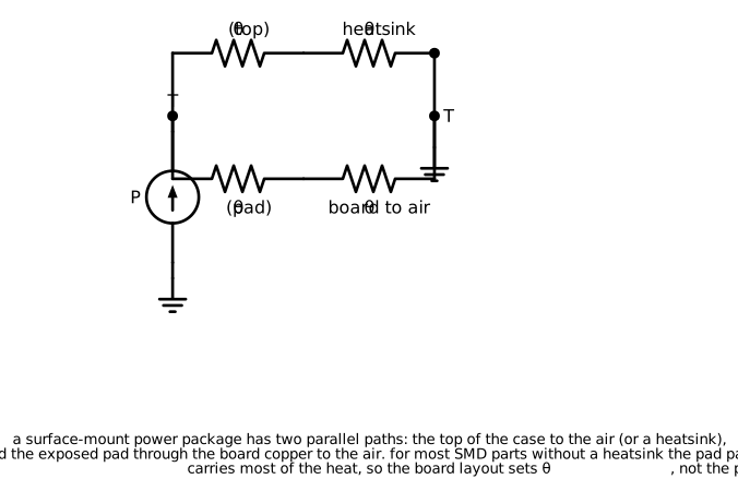 Figure 2. The two parallel paths out of a surface-mount power package: the top of the case to the air or a heatsink, and the exposed pad into the board.
A surface-mount package loses heat two ways in parallel: through the top of the mold compound to the air (or a heatsink on the top), and through the leads and the exposed pad into the board, which then loses it to the air from both faces. For a package with an exposed pad and no heatsink, the pad path carries most of the heat: θjc through the pad is often 1 to 5 °C/W while θjc through the top is 20 to 50 °C/W. The top path matters when a heatsink is attached to it, or for packages without an exposed pad.
Datasheets give both: θjc(top) and θjc(bottom) or θjb. The design uses the one for the path it is actually building.
The board as a heatsink
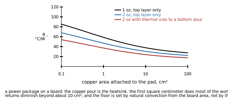 Figure 3. Junction-to-ambient thermal resistance versus the copper area attached to the pad, for 1 oz and 2 oz outer copper, and with thermal vias to a pour on the far side. The first square centimeter does most of the work.
For most boards without an external heatsink, the copper pour connected to the pad is the heatsink. The heat spreads laterally through the copper (which conducts about 400 W/mK) and then leaves the board surface by convection and radiation, at roughly 10 W/m²K for natural convection in free air. The board's FR-4 conducts about 0.3 W/mK, a thousand times worse than copper, so heat does not spread through the laminate; it spreads through copper and crosses the laminate only through vias.
The relationships:
- Copper area. θja falls quickly as the pour grows from the pad to about 1 cm², more slowly to 10 cm², and hardly at all beyond. Past a few square centimeters the limit is the spreading resistance of the thin copper, not the convection area.
- Copper thickness. 2 oz copper spreads heat about twice as far as 1 oz. For a pour that is much larger than the package, thicker copper makes more of it effective.
- Both sides. A pour on the far side, connected by thermal vias, roughly doubles the convecting area and shares the spreading between two layers. Internal planes connected by vias help spreading but do not convect.
- Board area. Once the pour is large, the whole board becomes the convecting surface. A 100 × 100 mm board in still air has a total surface thermal resistance around 10 °C/W; a 25 × 25 mm board around 60 °C/W regardless of copper.
- Airflow. Forced air at 1 m/s roughly halves the convective resistance; at 3 m/s it is a third.
- Neighbors. Two parts sharing a pour share its thermal resistance. The pour's rise is the total power times the pour's θ.
Rules of thumb for a 1 to 3 W package on a two-layer board in still air: 2 oz copper, at least 10 cm² of pour connected to the pad, the same area on the far side, and 9 to 25 thermal vias under the pad, gives a θja in the 25 to 40 °C/W range. Below that, an external heatsink, a metal-core board, or airflow is needed.
Thermal vias
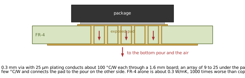 Figure 4. Cross-section of thermal vias under an exposed pad, carrying heat through the laminate to a pour on the far side.
A plated via is a copper tube through the board. Its thermal resistance along its length is
with l the board thickness, d the drill diameter, t the plating thickness, and k the conductivity of copper. For a 0.3 mm drill with 25 µm plating through 1.6 mm, that is about 170 °C/W per via; with the FR-4 in parallel and the via filled or capped, a design figure of about 100 °C/W per via is reasonable. An array of 16 vias is then around 6 °C/W, small compared with the rest of the path, which is the goal: the vias should not be the bottleneck between the pad and the far-side pour.
Practical guidance:
- Use 0.3 to 0.4 mm drills on a 1.0 to 1.2 mm pitch across the pad. Larger vias wick solder away from the pad during reflow and leave voids under the package.
- Tent or fill the vias when solder wicking is a concern; filled and capped vias (via-in-pad) are the cleanest solution and cost more.
- Connect the vias to a pour on the far side and to any internal ground planes. A via that ends on a small pad conducts to nothing.
- More vias help until their combined resistance is well below the spreading resistance of the pour. Beyond about 25 under a 5 mm pad the return diminishes.
- Keep the pad's pour connected on the top layer too; the top copper spreads heat away from the package before the vias carry it down.
Interface to the board
The solder joint between an exposed pad and its land is part of the path. A voided joint (from outgassing, from unfilled vias, or from a poor stencil design) raises θjc(bottom) substantially; 50 % voiding can double it. Stencil apertures for large pads are usually windowed (several smaller openings) to let flux escape. X-ray inspection of the pad joint is the check for a part that runs hotter than calculated.
External heatsinks
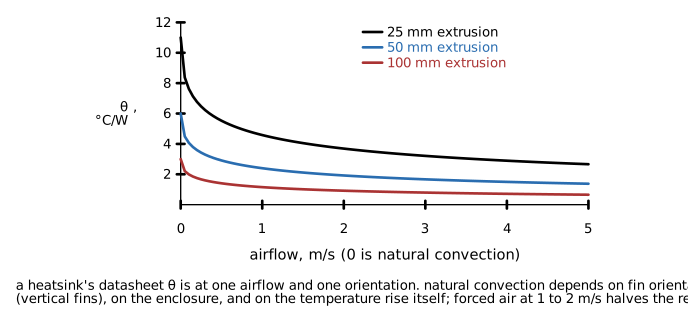 Figure 5. Heatsink thermal resistance versus airflow for three extrusion lengths. The datasheet value is at one airflow and orientation.
When the board cannot dissipate the power, a heatsink attaches to the package (for TO-220, TO-247, D2PAK with a top clip, or a module) or to a copper area with a thermal interface.
Sizing
Start from the allowed junction temperature and work outward:
with Tj,max derated from the absolute maximum (125 °C from a 150 °C rating is typical) and Ta the actual ambient inside the enclosure at the heatsink, not the room. The thermal chain calculator on the tools page does this arithmetic.
Heatsink data
A heatsink datasheet gives θsa under one condition, usually natural convection with the fins vertical and a specified temperature rise, or a curve against airflow. The value depends on:
- Orientation. Natural convection needs the fins vertical so air can rise between them. Horizontal fins, or a heatsink lying flat with fins up, can be 30 to 50 % worse.
- Airflow. Forced convection at 1 to 2 m/s halves the resistance relative to natural convection; the curve flattens above 3 to 4 m/s.
- Temperature rise. Natural convection and radiation both improve with rise, so a heatsink rated at 75 °C rise performs worse at 30 °C rise. Some datasheets give a correction curve.
- Enclosure. A heatsink inside a sealed box sees the box's internal air temperature, and the box wall becomes the final heatsink. Sealed enclosures with no external fins are limited to a few watts per hundred square centimeters of wall.
- Surface finish. Anodized (black or otherwise) surfaces radiate; bare aluminum does not. Radiation is a third of the natural convection performance of a small heatsink at typical rises.
Interface material
The case-to-sink resistance depends on the contact. Two machined surfaces touch at a few high points and trap air elsewhere; a thermal interface material fills the gaps.
| Interface | θcs for a TO-220 (about 1 cm²) | Notes |
|---|---|---|
| Dry, bare metal, good pressure | 1 to 2 °C/W | Air gaps dominate |
| Thermal grease, thin layer | 0.2 to 0.5 °C/W | Best performance; pumps out over thermal cycles, messy |
| Phase-change pad | 0.3 to 0.6 °C/W | Grease performance, handles like a pad |
| Silicone thermal pad, 0.5 mm | 0.8 to 2 °C/W | Easy, compliant, fills large gaps, poor conductivity |
| Insulating pad (mica, Kapton, ceramic) plus grease | 0.5 to 1.5 °C/W | When the tab must be isolated; ceramic best |
| Gap filler, 1 to 3 mm | 2 to 10 °C/W | For bridging to an enclosure wall; thickness dominates |
Mounting pressure matters for every option: the datasheet value assumes the specified torque or clip force. A pad that is too thin for the gap or too thick for the pressure performs far worse than its rating.
Isolation
A heatsink shared by several devices, or connected to chassis, must be electrically isolated from any tab at a voltage. The isolating pad adds θcs and capacitance (a TO-220 pad to a grounded heatsink is 10 to 50 pF), and for a switching device that capacitance is a common-mode noise path. Ceramic (alumina, aluminum nitride) isolators have the best thermal performance; a package with an isolated tab (full-pack or isolated-substrate types) avoids the problem at a higher θjc.
Transient thermal impedance
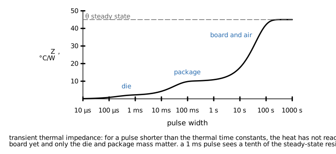 Figure 6. Transient thermal impedance versus pulse width. Short pulses see only the die and package; the board and air join at longer times.
Thermal resistance is the steady-state value. For power applied for a time shorter than the thermal time constants of the path, the heat has not reached the outer elements yet and the effective impedance is lower. The datasheet's transient thermal impedance curve, Zth(t), gives the effective junction-to-case (or ambient) impedance for a single pulse of width t, and usually a family of curves for repetitive pulses at various duty cycles.
Time constants, roughly: die, 0.1 to 1 ms; package, 10 ms to 1 s; board and heatsink, 10 s to minutes. A 100 µs pulse sees only the die and the effective impedance can be 1 to 5 % of the steady-state θja. A 10 s pulse sees nearly all of it.
Uses:
- Pulse ratings: a MOSFET's safe operating area in the pulsed region, a resistor's pulse capability, an LED's peak current.
- Duty-cycled loads: for a pulse train at duty D with period T, the peak junction rise is approximately P·[D·θ + (1 - D)·Zth(T)], read from the repetitive-pulse curves.
- Fault survival: a short-circuit or an inrush lasts milliseconds; the junction temperature during it is set by Zth at that width, not by θja.
The Zth curve is a package-and-mounting property and is given for the datasheet's test condition; for short pulses it is nearly independent of the board, for long ones it is the board's.
Measuring junction temperature
The design is verified by measurement, because the model's uncertainty is large.
- Thermocouple on the case. A fine-gauge (36 to 40 AWG) thermocouple bonded to the top of the package, with the leads run along an isotherm, reads the case temperature. Add P·θjc for the junction. A large thermocouple or one pointing away from the surface reads low by tens of degrees.
- Infrared camera. Reads surface temperature of high-emissivity surfaces (mold compound, black paint); bare metal and shiny surfaces read low. Useful for finding the hot spot and for pours; needs an emissivity setting or a spot of matte tape.
- Temperature-sensitive parameter. Many devices have an internal thermometer: the forward voltage of a body diode or an ESD diode at a small current (about -2 mV/°C), an on-die temperature sensor readable over I2C, or the RDS(on) of a MOSFET. This reads the junction directly and is the reference method.
- Board-level: a thermistor on the pour or a temperature sensor IC gives the board temperature that the θjb model needs.
Measurements are made at the worst-case ambient, in the enclosure, at full power, after thermal equilibrium (which can take 20 to 60 minutes for a heatsinked assembly), and at the highest input voltage or whatever condition maximizes dissipation.
Reading the datasheet
- θjc, and for which surface (top or bottom). Only this is a package property.
- θjb, if given, for the board-cooled case.
- θja and the JEDEC board it was measured on (1s0p, 2s2p, and the copper area). Use it to compare packages, not to design.
- Zth curves for pulsed operation.
- Maximum junction temperature and any derating of the electrical ratings with temperature (current, RDS(on), gain).
- Recommended land pattern with thermal via pattern, which is the vendor's tested configuration.
Design procedure
- Determine the power dissipated in the part at the worst case: maximum load, maximum input voltage or minimum efficiency, and highest ambient. Include switching loss, gate drive, quiescent current, and transient conditions.
- Set the junction temperature limit with margin (typically 20 to 25 °C below the absolute maximum, more for a long-life product).
- Determine the ambient at the part: the air inside the enclosure at the worst case, not the room. If unknown, estimate the enclosure rise from the total dissipation and the enclosure surface, and add it.
- Compute the required θja from junction to that ambient.
- Choose the path: board only, board plus airflow, top-side heatsink, or a metal-core board. For a board path, choose copper area, thickness, vias, and far-side pour to meet the target using the vendor's application data (most power IC datasheets give θja versus copper area on their own test board).
- For a heatsink path, compute θsa,required and select a heatsink with margin at the actual airflow and orientation. Select the interface and the mounting hardware.
- Check pulsed and transient conditions against Zth.
- Lay out the board with the thermal path in mind: pour on both sides, vias under the pad, heat-generating parts spaced apart and away from temperature-sensitive ones, and the heatsink mounting mechanically sound.
- Build, measure at worst case, and compare with the model. Adjust.
Worked example: a 3 W regulator on a board
A synchronous buck controller with integrated FETs in a 5 × 5 mm QFN with an exposed pad dissipates 2.4 W at full load, 12 V in, at an enclosure ambient of 55 °C. The datasheet gives θjc(bottom) 2 °C/W, θja 32 °C/W on a JEDEC 2s2p board, and Tj,max 150 °C. The product board is two-layer, 60 × 40 mm, 1 oz copper.
Target. Tj limited to 120 °C. Required θja = (120 - 55) / 2.4 = 27 °C/W. This is already below the JEDEC figure on a better board than the product has, so a plain layout will not meet it.
Board path estimate. Two-layer, 1 oz, 8 cm² pour top and bottom, 16 vias: from the vendor's copper-area curve and Figure 3, about 45 °C/W. Tj = 55 + 2.4 × 45 = 163 °C. Fails.
Options.
- 2 oz copper both sides with the same pour: about 35 °C/W. Tj = 139 °C. Fails the 120 °C target, passes the absolute maximum with no margin.
- 2 oz copper and the pour extended to the full board (24 cm² each side): about 28 °C/W. Tj = 122 °C. Marginal.
- Option 2 plus a 12 × 12 mm stick-on heatsink on the top of the package: the top path adds a parallel branch of θjc(top) 20 °C/W plus 25 °C/W for a small heatsink in still air, 45 °C/W in parallel with 28 gives 17 °C/W. Tj = 96 °C. Passes with margin.
- Reduce the dissipation: raising the switching frequency changes little, but a lower input voltage or a different controller with lower RDS(on) at 1.6 W dissipation would give Tj = 55 + 1.6 × 28 = 100 °C on option 2 alone.
Option 3 is chosen for the existing part, with the fallback of option 4 at the next revision. The design is verified by measuring the case top with a fine thermocouple at 55 °C ambient in the enclosure at full load; the predicted case temperature is Tj - P·θjc(top path share), and a measured value more than 10 °C above the prediction triggers an X-ray of the pad joint.
Design errors
- Datasheet θja used to predict Tj on a small board. Correction: use θjc or θjb with a board estimate from the vendor's copper-area data, then measure.
- Exposed pad without vias, or vias without a far-side pour. Correction: 9 to 25 vias to a pour on the other side.
- Pour on the top layer only, 1 oz, isolated by a thermal relief. Correction: thermal reliefs off on the pad connection; full connection to the pour, 2 oz, both sides.
- Room ambient used for the calculation. Correction: enclosure ambient at the part, measured or estimated from the enclosure's total dissipation.
- Heatsink chosen from its still-air rating and mounted with fins horizontal in a sealed box. Correction: orientation, enclosure temperature, and the rise-dependence all applied; verify by measurement.
- Thermal pad specified without a pressure or a gap tolerance. Correction: specify pad thickness against the gap range and the clip or screw force.
- Pulsed load sized on average power. Correction: Zth at the pulse width; if the pulse is longer than the thermal time constant, size on the pulse power.
- Two power parts sharing one pour, each calculated alone. Correction: total power into the shared pour; separate pours if the rise is too high.
- Junction temperature inferred from a thermocouple on the heatsink. Correction: add P·(θjc + θcs), or measure a temperature-sensitive parameter.
- Thermal design left until the layout is done. Correction: the pour area, via array, and heatsink mounting are placement constraints from the start.
Limitations of this document
- Thermal resistance values in the tables and figures are typical ranges for illustration. The package datasheet, the vendor's application note for the board configuration, and a measurement govern.
- The lumped-resistance model does not capture spreading in detail, temperature-dependent convection, or radiation between parts. It predicts to a factor of two at best when the resistances are estimated.
- Forced-air and enclosure-level design (fan selection, pressure drop, air routing) are outside the scope.
- Metal-core boards, direct-bonded copper substrates, and embedded heat spreaders are not covered.