ESD, Surge, and Protection
noteProtecting a board's external interfaces: what an ESD event and a surge actually are (IEC 61000-4-2 and 61000-4-5 waveforms and levels), the difference between standoff, breakdown, and clamping voltage, TVS and other clamp devices compared, two-stage protection with a series element, where the clamp goes on the board and why placement decides everything, protecting power inputs and data lines, ground strategy at the connector, EFT, and a selection procedure with worked examples.
related tools: creepage & clearance (iec 60664-1, ipc-2221b)
Scope: transient protection at the interfaces of a product, from electrostatic discharge through the connector to lightning-induced surge on a cable. The note covers the standard test events, the protection devices and their parameters, the circuit topology, the board placement and grounding that make protection work, and selection. Device-level (HBM, CDM) ESD of bare ICs, mains surge protection at the service entrance, and lightning direct strikes are outside the scope.
Common errors
- Choosing a TVS by its standoff voltage. The circuit sees the clamping voltage at the surge current, which is typically 1.5 to 2 times the standoff. A 5 V standoff part clamps at 9 to 10 V.
- Placing the TVS near the IC instead of at the connector. The surge current then travels across the board before it is clamped, and the inductance of that path adds volts per nanosecond to what the IC sees.
- Long ground return from the TVS. A clamp is only as good as its ground path. 10 mm of trace is 10 nH, which is 100 V at 10 A/ns.
- One-stage protection. A TVS alone at a 5 V line clamps to 10 V at ESD current; a 3.3 V IC pin does not survive 10 V. A series element after the clamp turns the residual voltage into a current the IC's own diodes can handle.
- Using an ESD diode array for surge. A part rated for 8 kV ESD absorbs microjoules. A 1 kV surge delivers tens of joules; the array becomes a short and then an open.
- Protecting the signal and forgetting the shield, the ground, and the power. The event enters through whatever path has the lowest impedance, which is often not the signal pin.
- Adding protection after the layout is done. The clamp and its ground path define the connector region's layout; they cannot be appended.
- Passing the test on the bench and failing in the field. The test discharges are to defined points; a product in the field is discharged to whatever the user touches, including seams and screws.
What the events are
Electrostatic discharge (IEC 61000-4-2)
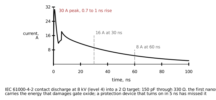 Figure 1. IEC 61000-4-2 contact discharge current at 8 kV into the calibration target. The first nanosecond carries the peak; the tail lasts a hundred nanoseconds.
A person charged by walking across a carpet carries a few kilovolts on about 150 pF of body capacitance and discharges it through about 330 Ω of skin and contact resistance. IEC 61000-4-2 models this with a generator of those values, applied to the product either by contact discharge (the probe tip touching a conductive point, the reference method) or by air discharge (a charged probe approaching an insulating surface until it arcs, used for non-conductive surfaces).
| Level | Contact discharge | Air discharge | Peak current (contact) |
|---|---|---|---|
| 1 | 2 kV | 2 kV | 7.5 A |
| 2 | 4 kV | 4 kV | 15 A |
| 3 | 6 kV | 8 kV | 22.5 A |
| 4 | 8 kV | 15 kV | 30 A |
The current waveform is the defining fact: a peak of 3.75 A per kilovolt within 0.7 to 1 ns, then a slower body of 2 A per kilovolt at 30 ns and 1 A per kilovolt at 60 ns. The total energy at 8 kV is about 5 mJ. The damage mechanism is voltage across gate oxide (a few volts of overstress ruptures a thin oxide) and current density in a junction (a few amps for a few nanoseconds melts a small junction). The energy is small; the rise time is the problem, because any inductance in the protection path turns the di/dt into voltage.
Consumer and industrial products are typically tested to level 3 or 4 (6 or 8 kV contact, 8 or 15 kV air), with performance criteria: A (no effect), B (temporary degradation, self-recovering), C (needs a reset), D (damage). A product usually needs criterion B for ESD.
Surge (IEC 61000-4-5)
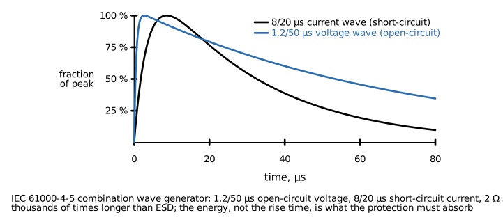 Figure 2. IEC 61000-4-5 combination wave: the 1.2/50 µs open-circuit voltage and the 8/20 µs short-circuit current.
Surge models the effect of nearby lightning or switching of large loads: a voltage induced into cables and power lines. The combination wave generator delivers a 1.2/50 µs voltage into an open circuit and an 8/20 µs current into a short, with an effective source impedance of 2 Ω; coupling networks add 10 to 42 Ω depending on the port (12 Ω for power line-to-line with the 10 Ω network, 42 Ω for signal lines and for line-to-earth).
| Level | Open-circuit voltage | Short-circuit current at 2 Ω |
|---|---|---|
| 1 | 0.5 kV | 250 A |
| 2 | 1 kV | 500 A |
| 3 | 2 kV | 1000 A |
| 4 | 4 kV | 2000 A |
The energy is thousands of times larger than ESD: at 1 kV through a 42 Ω network a signal line sees about 24 A for tens of microseconds, roughly 10 to 20 mJ into a clamp; a power port at 2 kV with the 12 Ω network delivers 170 A and several joules. Rise time is a microsecond, so inductance in the path matters less; the challenge is absorbing and surviving the energy. Surge is applied with positive and negative polarity, at several phase angles for AC ports, five pulses each, and the product typically needs criterion B on signal ports and A or B on power.
Electrical fast transient (IEC 61000-4-4)
EFT models the arcing of relay and switch contacts: bursts of 5/50 ns pulses at 5 kHz or 100 kHz repetition, 0.5 to 4 kV, coupled capacitively onto cables (a clamp around the cable bundle) or directly onto power ports through 33 nF. The individual pulse energy is small; the problem is the repetition and the common-mode coupling into every conductor at once. EFT failures are usually resets and communication errors rather than damage, and the fixes are common-mode filtering, shield termination, and firmware robustness rather than clamps.
Other transients
- Cable discharge event (CDE): a long cable (Ethernet, USB) charged by handling discharges into the port on connection. Peak currents exceed ESD because the cable's capacitance is larger and its impedance lower.
- Hot plug: connecting a live supply into a capacitive input; inrush current and, through cable inductance, an overshoot of up to twice the supply voltage.
- Load dump (ISO 7637-2, ISO 16750): in a vehicle, disconnecting the battery from a charging alternator produces a 40 to 100 V pulse lasting hundreds of milliseconds with an energy of joules. This requires a dedicated power TVS or an active clamp.
- Inductive kickback: a relay or motor coil switched off produces a voltage spike limited only by the switch's breakdown, which is protected at the coil with a diode, a TVS, or an RC.
Protection devices
TVS diodes
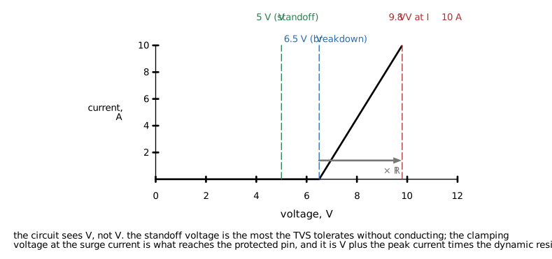 Figure 3. The V-I curve of a unidirectional TVS. Standoff voltage is the most it tolerates without conducting; breakdown is where it starts; clamping voltage at the rated pulse current is what the circuit sees.
A transient voltage suppressor is an avalanche diode built for pulse current. Its parameters:
| Parameter | Symbol | Meaning |
|---|---|---|
| Reverse standoff voltage | VRWM | Maximum continuous voltage with only leakage current. Must exceed the normal operating voltage including tolerance and ripple. |
| Breakdown voltage | VBR | Voltage at a small test current (1 mA) where conduction begins. Typically 1.1 to 1.3 × VRWM. |
| Clamping voltage | VC | Voltage at the rated peak pulse current IPP. This is what the protected circuit sees. Typically 1.3 to 1.6 × VBR. |
| Peak pulse current | IPP | The 8/20 µs (or 10/1000 µs) current at which VC is specified. |
| Peak pulse power | PPP | IPP × VC at the specified waveform; 400 W to 30 kW for surge parts, given at 10/1000 or 8/20 µs. |
| Dynamic resistance | Rdyn | Slope of the V-I curve in conduction; VC ≈ VBR + IPP × Rdyn. Lower is better; 0.1 to 1 Ω for surge parts. |
| Capacitance | CJ | Junction capacitance at zero bias, from 0.2 pF (signal parts) to nanofarads (power surge parts). |
| Leakage current | IR | At VRWM; microamps to milliamps, rising with temperature. |
| ESD rating | IEC 61000-4-2 level the part survives, for signal-line parts; often 15 to 30 kV. |
Unidirectional parts clamp in one polarity by avalanche and conduct as a forward diode (about 1 V) in the other; they suit DC rails and single-polarity signals and clamp negative transients hard. Bidirectional parts are two avalanche junctions back to back for AC or bipolar signals.
Two families serve different jobs:
- Surge TVS (SMA, SMB, SMC, DO-214, larger): watts to kilowatts of peak power, capacitance in the hundreds of picofarads to nanofarads, for power inputs and low-speed lines. Specified for 8/20 or 10/1000 µs.
- ESD protection diodes (SOD-923, DFN, arrays): capacitance of 0.2 to 5 pF for data lines, low clamping voltage, rated for IEC 61000-4-2 and sometimes for a small 8/20 µs current (a few amps). They absorb ESD energy and not surge energy.
Deep-snapback and silicon-controlled-rectifier-based ESD devices clamp lower than a simple diode by switching to a low-voltage state, at the cost of a holding current that must be above the line's normal current to avoid latch-up.
Other devices
| Device | Strengths | Limits | Use |
|---|---|---|---|
| Metal oxide varistor (MOV) | Joules of energy, cheap, high voltage | High clamping ratio (2 to 3 × rated), degrades with each surge, high capacitance, fails short | AC mains, high-energy DC, load dump |
| Gas discharge tube (GDT) | Very high current (kA), near-zero capacitance | Slow to fire (hundreds of volts, microseconds), follow-on current on DC lines | Telecom, outdoor lines, primary protection ahead of a TVS |
| Thyristor surge protector (TSS, SIDACtor) | Crowbar, low clamped voltage, high current | Holding current, must be able to turn off | Telecom, PoE |
| Polymer ESD suppressor | Very low capacitance | Higher trigger voltage, wears with events | High-speed lines where a diode's capacitance is too much |
| Series resistor | Limits current into the protected pin, no energy limit | Adds resistance in the signal path | Secondary protection on every signal that can afford it |
| Ferrite bead | Impedance to the fast edge, converts to heat | Saturates, low impedance below 10 MHz | Secondary protection, EFT |
| Spark gap on the board | Free, zero capacitance | Arcs at 1 to 3 kV depending on gap and coating, not reliable, prohibited by some standards | Last resort on cheap products; unreliable with conformal coat |
| Common-mode choke | Attenuates common-mode EFT and ESD | No clamping | Cable ports, in front of the clamp |
| Fuse or PTC | Limits sustained fault current after the clamp fails short | Slow | Always with a clamp that fails short on a power line |
Coordination
When more than one device is on a line, they must share correctly. A GDT in front of a TVS must fire before the TVS is destroyed, which requires a series impedance (a resistor or the cable's own inductance) between them so that the voltage across the GDT rises to its firing voltage while the TVS carries the initial current. A MOV in parallel with a TVS does not share: the TVS clamps first and absorbs everything until it fails. Coordination is a design step, not an accident.
Protection topology
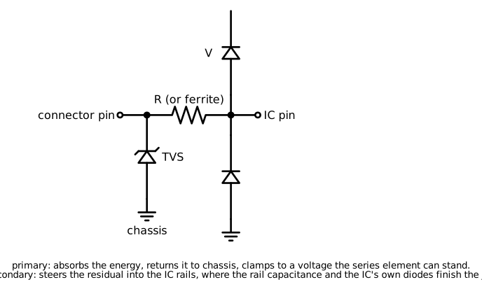 Figure 4. Two-stage protection. The primary clamp absorbs the energy at the connector; the series element limits current; the secondary steers the residual into the rails at the IC.
A single clamp cannot both survive the event and clamp low enough for a modern IC. The solution is two stages separated by an impedance:
- Primary clamp at the connector: a TVS (or MOV or GDT for high energy) rated for the event, clamping to a voltage the series element and the secondary can withstand, returning the current to chassis ground.
- Series element: a resistor (10 Ω to 1 kΩ, sized against the signal's bandwidth and current), a ferrite bead, or the cable's inductance. It converts the residual clamp voltage into a limited current.
- Secondary clamp at the IC: a low-capacitance diode array to the rails or a low-voltage TVS. It absorbs what the series element lets through, which is a fraction of an amp. The IC's own protection diodes are the last stage, rated for a few amps for nanoseconds and nothing for microseconds.
The rails the secondary steers into must be able to absorb the charge: the rail's bulk capacitance takes it, and a rail with a small capacitor and a regulator that cannot sink current will rise. A TVS on the rail, or a diode from the rail to a larger rail, bounds it.
For power inputs the same structure applies with different parts: a fuse or PTC, then a surge TVS or MOV to ground, then the input filter's inductor as the series element, then the input capacitors and the regulator's own rating. Reverse polarity protection (a series diode, a P-channel FET, or a shunt diode with a fuse) belongs in the same block.
Placement and layout
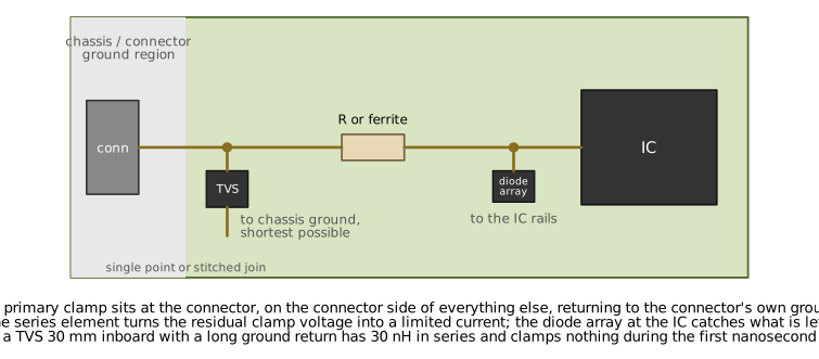 Figure 5. Placement at the connector. The primary clamp sits on the connector side of everything, returning to the connector's ground; the series element and the secondary follow.
Placement decides whether the protection works, because ESD current has a di/dt of 30 A/ns and every nanohenry in the path produces 30 V:
- The primary clamp goes at the connector, on the connector side of every other component on the line, within a few millimeters of the pin. A clamp 30 mm inboard clamps the point 30 mm inboard; the traces between it and the connector, and anything coupled to them, see the full event.
- The clamp's ground return goes to the connector's ground, the shortest and widest possible, to a chassis or connector ground region. A via to a plane is 1 nH; a 10 mm trace is 10 nH. The current must return to where it came from, which is the connector shell, the cable shield, or the chassis, not the circuit ground on the far side of the board.
- Chassis and circuit ground meet in one place. The connector region has its own ground (chassis, or a ground island tied to chassis at the connector) so that the surge current flows connector to clamp to chassis without crossing the circuit ground. The circuit ground connects to it at one point, or through stitching near the connector, or through a capacitor for a floating design. Surge current flowing across the circuit ground plane shifts the ground under every IC on its path.
- Keep protected and unprotected traces apart. The trace between the connector and the clamp carries the full event; a trace routed next to it, or over a split under it, picks it up.
- Keep the series element between the stages, not before the primary (where it would carry the full current) and not after the secondary (where it does nothing).
- Route the signal through the clamp's pad, or as close as the footprint allows, rather than on a stub to the clamp. A stub adds inductance to the clamp path.
- Provide a discharge path for every conductive surface a user can touch: connector shells, screws, metal buttons, and enclosure seams need a bond to chassis, or a clearance to internal circuitry that exceeds the air discharge test voltage (about 1 mm per kilovolt, 8 mm for 8 kV, more with sharp points).
- Unprotected pins are not protected. Every pin on an external connector needs a path, including unused pins (tie to ground or leave with clearance), shield pins, and power pins.
For surge, the same geometry applies with less sensitivity to inductance and more to the current-carrying capacity of the traces: a 500 A, 20 µs pulse through a 0.2 mm trace lifts it.
Protecting specific interfaces
| Interface | Threat | Primary | Series | Secondary and notes |
|---|---|---|---|---|
| DC power input, 12 to 48 V | Surge, reverse polarity, hot plug, load dump | Surge TVS sized for the level and the impedance network, or MOV; fuse before it | Input filter inductor or a resistor for low power | Input capacitors; regulator with an input rating above VC; reverse polarity FET |
| USB 2.0 | ESD, CDE | Low-capacitance ESD array on D+, D-, VBUS at the connector | Ferrite or 0 Ω on VBUS, none on data (impedance) | Controller's own protection; VBUS TVS |
| USB 3, HDMI, DisplayPort, PCIe | ESD | Ultra-low-capacitance (below 0.5 pF) arrays or polymer, matched to the pair | None | Layout for impedance continuity through the array |
| Ethernet | Surge (common mode), ESD | Magnetics provide isolation; Bob Smith termination and chassis capacitor on the cable side; TVS on the line side of the magnetics for PoE | The transformer itself | PHY-side ESD array; PoE needs surge TVS on the PD input |
| RS-232, RS-485, CAN | ESD, surge, EFT | Bidirectional TVS sized for the bus's common-mode range (RS-485 -7 to +12 V, CAN ±12 V or more) | 10 Ω resistors, or the transceiver's own isolation | Transceivers with integrated ±15 kV ESD; for surge, transceivers rated for it plus the TVS |
| Analog inputs (sensors, 4 to 20 mA) | ESD, surge on long cables | TVS at the connector, GDT for outdoor lines | 1 kΩ or more (the input is high impedance) | Clamp diodes to the rails at the amplifier; the resistor limits current to what they take |
| Digital GPIO to a panel or cable | ESD, EFT | ESD diode at the connector | 100 Ω to 1 kΩ | IC diodes |
| Antenna port | ESD | Shunt inductor (DC short, RF open) or a very low-capacitance diode | None | Match must survive the diode's capacitance |
| Buttons and touch surfaces | Air discharge | ESD diode at the switch, or clearance | Series resistor | Firmware debounce that ignores glitches |
Ground and shield strategy
The event's current must have somewhere to go that is not through the circuit. Three arrangements:
- Chassis grounded product with a metal enclosure: the shield, the connector shells, and the primary clamps return to the chassis at the connector. The board's ground connects to chassis at the connector region, so that the surge current does not traverse the board.
- Plastic enclosure, no chassis: there is no chassis to return to, and the event current returns through the cable's own conductors or through capacitance to the environment. The connector region's ground island is tied to the board ground at one point and the clamps return there; the board itself is the "chassis". A larger board ground area helps, and a capacitor (Y-rated where mains is involved) from the ground island to any internal metal spreads the discharge.
- Isolated ports: the port is isolated from the board (transformer, optocoupler, isolator IC) and the port-side ground is a small island. Protection on the port side returns to the island; the isolation barrier's rating (working voltage and transient) must exceed the surge, and the capacitance across the barrier sets how much common-mode transient couples through.
In all cases: the primary protection's return path must never be the signal ground plane under the ICs.
Testing
A design is confirmed by test, on the product as built, with the intended enclosure and cables:
- ESD per IEC 61000-4-2 with a calibrated gun, contact discharge to every conductive point a user can reach, air discharge to every insulating surface, both polarities, ten discharges each, plus indirect discharge to the horizontal and vertical coupling planes. Watch for resets and communication errors (criterion B failures), not only damage.
- Surge per IEC 61000-4-5 with the coupling network for each port type, both polarities, five pulses at each phase angle for AC.
- EFT per IEC 61000-4-4 with the capacitive clamp on each cable bundle.
- Before formal testing, a bench ESD gun on the prototype connector region, with a scope on the protected node and a current probe on the ground return, shows where the current goes and what the IC actually sees.
Diagnosis when a test fails: identify the entry point (which discharge point, which cable), then the path (where the current flows through the board, found by moving the discharge point and by current-probing ground connections), then the victim (usually a reset line, a clock, an enable pin, or a high-impedance analog node coupled to the path). The fix is at the entry point and the path, not at the victim.
Selection procedure
- List every external conductor: signal pins, power, ground, shield, connector shell, and every conductive or touchable surface.
- Determine the test levels and criteria from the product's standard (generic industrial, IEC 61000-6-2; medical, IEC 60601-1-2; automotive, ISO 10605 and ISO 7637; consumer, EN 55035), and any customer requirements.
- For each line, determine the normal operating voltage range including tolerances, ripple, and any signaling above the rail. The primary clamp's standoff must exceed this.
- Determine the maximum voltage the next stage can survive (the series element's rating, the secondary's, the IC's absolute maximum), and the current the IC's diodes can take.
- Choose the primary device type by energy (ESD array for ESD only; surge TVS or MOV for surge; GDT plus TVS for outdoor or telecom) and by capacitance for the signal's speed.
- Compute the clamping voltage at the event current: VC = VBR + IPP × Rdyn. Confirm the series element and secondary handle it, and that the residual current into the IC is within its rating.
- Check the primary's pulse rating against the event with margin, including repetition (the standard applies multiple pulses) and temperature derating.
- Check leakage at the operating voltage and temperature against the circuit's tolerance, and capacitance against the signal.
- Place the devices per the layout rules, and design the connector ground region.
- Add a fuse or PTC on any power line where the clamp's short-circuit failure would otherwise be a fire.
- Test on the prototype with a gun and a scope, then formally.
Worked examples
RS-485 port, industrial, 2 kV surge and 8 kV ESD
The transceiver has ±15 kV ESD protection integrated but a surge rating of only ±1 kV through a 42 Ω network, and an absolute maximum of -8 to +13 V on the bus pins. The bus common-mode range is -7 to +12 V.
- Primary: a bidirectional surge TVS with VRWM ≥ 12 V; a 15 V bidirectional SMB part, VBR 16.7 V, IPP 24 A at VC 22 V for 8/20 µs (a 600 W part). At 2 kV through 42 Ω the current is about 43 A; a 1500 W SMC part with VC 24 V at 43 A is selected, one across A to ground and one across B to ground (or A to B plus a common-mode pair, depending on the coupling mode tested).
- Series: 10 Ω pulse-rated resistors (thick film, 2010 size or a pulse-rated MELF, rated for the 24 V / 10 Ω = 2.4 A for 20 µs) in each line between the TVS and the transceiver. They drop the transceiver's residual current to a few amps for microseconds, within the transceiver's rating, and cost 20 mV of signal at 2 mA.
- Secondary: the transceiver's own ±15 kV ESD structures.
- Layout: TVS within 3 mm of the connector pins, returning to a chassis ground fill under the connector, stitched to chassis via the connector's mounting holes; the board ground joins that fill at one point.
- The 10 Ω resistors add 20 Ω to the bus; with a 120 Ω termination the driver still meets the RS-485 load, and for a long bus the series resistance is checked against the receiver threshold budget.
24 V DC power input, industrial, 1 kV surge line-to-line, 2 kV line-to-earth
The regulator's input rating is 42 V; the operating voltage is 24 V ± 20 % (19 to 29 V) with possible 36 V transients from the supply.
- Fuse: a 2 A slow-blow, rated for the surge current without opening (the I²t of the 8/20 µs pulse is checked against the fuse's melting I²t).
- Primary: a 36 V unidirectional surge TVS, VBR 40 V, 1500 W. At 1 kV through 12 Ω the pulse current is 80 A; VC at 80 A from the datasheet is 52 V, above the regulator's 42 V rating. Two options: a 3 kW part with lower Rdyn (VC 46 V, still over), or a series element. A 10 µH input inductor is already present for EMI; its impedance to the 8/20 µs pulse limits the current into the input capacitors, and 100 µF of input capacitance at 80 A for 20 µs rises by 16 V. The combination keeps the regulator input below 42 V, confirmed by simulation and then by test. An alternative is a regulator rated to 60 V.
- Line-to-earth: the 24 V return is bonded to chassis at the connector, and the TVS returns there; the 2 kV pulse appears across the isolation of the supply, not across the regulator.
- Reverse polarity: a P-channel FET in the positive line after the fuse, with its gate protected by a 12 V zener and 100 kΩ.
- Layout: fuse, TVS, and FET at the connector on the chassis ground fill; the inductor after them; the regulator downstream.
USB 2.0 device port, consumer, 8 kV contact and 15 kV air
- Primary: a four-channel ESD array with 1 pF per channel (D+, D-, VBUS, ID) at the connector, rated ±15 kV air and contact, clamping D+ and D- to about 8 V at 8 kV and VBUS to about 10 V.
- VBUS: a 5.5 V standoff TVS in SOD-923 at the connector in addition, since VBUS carries the CDE current and the ESD array's VBUS channel is small; a ferrite bead between the connector VBUS and the internal 5 V rail.
- Data: no series element (the 90 Ω differential impedance would be spoiled); the controller's own ESD protection is the secondary, and the array's clamp is low enough.
- Shell: the connector shell bonds to chassis, or in a plastic product to the board ground island under the connector through a 1 MΩ resistor in parallel with a 4.7 nF capacitor, so that the shell discharges but does not carry the board ground out.
- Layout: the array on the D+/D- traces at the connector with the pairs routed through its pads, ground pins via to the ground island, and the island stitched to the board ground at the connector.
Design errors
- TVS chosen by standoff; the IC receives VC. Correction: compute VC at the event current; add a series element and secondary stage.
- ESD array on a surge-exposed line. Correction: surge TVS as primary, array as secondary.
- Clamp located at the IC. Correction: at the connector, on the connector side of everything.
- TVS ground returned through the signal ground plane. Correction: chassis or connector ground island, shortest path, single-point join to the board ground.
- Unused connector pins left floating and unprotected. Correction: tie or protect every pin.
- Power line MOV or TVS without a fuse. Correction: fuse or PTC upstream; the clamp fails short.
- Series resistor before the primary clamp. Correction: between the primary and the secondary.
- Capacitance of the protection ignored on a high-speed line. Correction: sub-picofarad array or polymer, placed for impedance continuity.
- Bench test only to the connector pins. Correction: test every touchable point, seams and screws included, and the air discharge on plastic surfaces.
- Reset and communication errors dismissed as "not damage". Correction: criterion B requires self-recovery; a reset is a failure for most products.
Limitations of this document
- Test levels, coupling networks, and performance criteria are summarized from IEC 61000-4-2, -4-4, and -4-5 and the generic standards; the applicable product standard governs.
- Device parameters are typical for the families named; the datasheet governs, and clamping voltage in particular varies with pulse width and temperature.
- The worked examples are sized to illustrate the method; the values are not a qualified design for any specific product.
- Mains-connected surge protection (service entrance, Type 1 and 2 SPDs) and lightning protection of outdoor equipment are outside the scope.