Digital Interfaces
noteThe electrical side of the common board-level and short-cable buses: I2C pull-ups, bus capacitance and rise time; SPI modes, clock rates and signal integrity; UART framing, baud error and levels; RS-485 termination, biasing and grounding; CAN termination and arbitration; level shifting between voltage domains; and the bring-up failures each one produces and how to find them with a scope.
related tools: i2c pull-up resistors
Scope: the electrical requirements of I2C, SPI, UART, RS-485, and CAN as they appear on a board or a short cable, and the failures that show up when a design is first powered. The note covers the physical layer, termination, pull-ups, voltage levels and level translation, timing at the edge level, and a bring-up checklist per bus. Protocol details (addressing, framing above the byte, error handling in software) are covered only where they explain an electrical symptom. USB, Ethernet, and high-speed serial links are outside the scope.
Common errors
- I2C pull-ups chosen by habit. 4.7 kΩ is correct for a short bus at 100 kHz and 3.3 V. It is wrong for a fast-mode bus with 200 pF of cable capacitance (too slow) and wrong for a 1.8 V bus with a weak sink (too strong).
- SPI run at the peripheral's maximum clock over a long trace or a ribbon cable. The clock edges ring, the peripheral samples the ringing, and the failure is intermittent.
- SPI mode assumed. Two devices on the same bus can need different CPOL and CPHA. A wrong mode shifts the data by one bit and is often invisible on a logic analyzer set to the wrong mode too.
- UART baud rate derived from a clock that cannot divide to it. A 3 % error per side is the whole budget; an 8 MHz crystal at 115200 baud is 3.5 % off.
- RS-485 with no termination, or termination at every node, or no ground wire. Each is a distinct failure with a distinct symptom.
- CAN without both terminations. The bus works on the bench with two nodes a meter apart and fails in the installation.
- Voltage domains crossed without translation. A 5 V open-drain I2C device on a 3.3 V bus works until the day it does not; a 5 V push-pull output into a 3.3 V input works until the input is damaged.
- Debugging with a logic analyzer only. The analyzer shows the digital interpretation of an analog waveform. Rise times, ringing, ground bounce, and marginal levels are visible only on a scope at the pin.
I2C
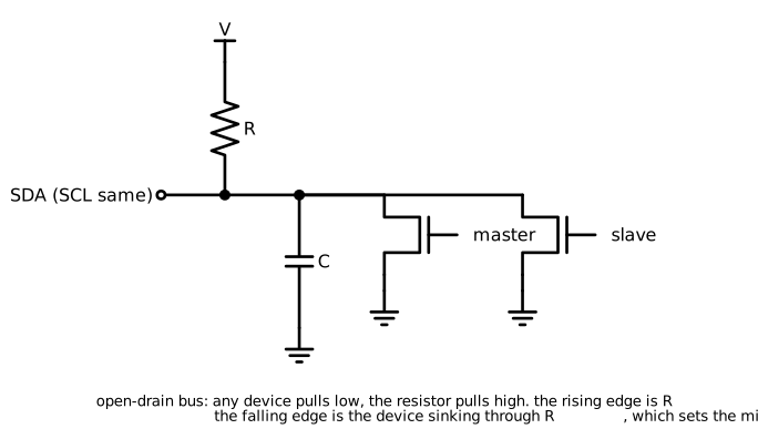 Figure 1. The I2C bus. Every device pulls low through an open-drain transistor; a single pull-up per line pulls high. The rise time is set by the pull-up and the bus capacitance.
I2C is a two-wire, open-drain, multi-drop bus: SDA and SCL, each with one pull-up resistor, driven low by any device and released to be pulled high by the resistor. The open-drain structure allows any number of devices, clock stretching, and multi-master arbitration, and it makes the rising edge the slowest thing on the bus.
Pull-up sizing
Two constraints bound the pull-up:
- Minimum resistance from the sink current. The specification requires a device to pull the line to 0.4 V while sinking 3 mA (standard and fast mode; 20 mA for fast-mode plus). So
which is 967 Ω at 3.3 V and 1.5 kΩ at 5 V. Some devices are specified for less than 3 mA; the weakest sink on the bus sets the limit.
- Maximum resistance from the rise time. The rise time is measured from 30 % to 70 % of Vcc and must be under 1000 ns (standard mode, 100 kHz), 300 ns (fast mode, 400 kHz), or 120 ns (fast-mode plus, 1 MHz):
With Cb the total bus capacitance (every device's pin capacitance, typically 10 pF each, plus trace at about 1 pF per centimeter and cable at 50 to 100 pF per meter), limited to 400 pF by the specification. For 100 pF and fast mode, Rp,max is 3.5 kΩ. The I2C pull-up calculator on the tools page evaluates both limits.
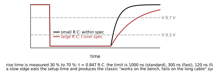 Figure 2. Rising edges with a correctly and an excessively large pull-up time constant. The rise time is measured between the 30 % and 70 % levels.
A pull-up near the minimum gives the fastest edge and the highest power (Vcc²/Rp while low, several milliwatts at 5 V and 1 kΩ) and the most stress on weak drivers. A pull-up near the maximum saves power and produces a slow edge that eats the setup time; devices see the level cross their input threshold late, and the bus works at a lower clock than intended or fails on the longest cable. A value between the limits, biased toward the low end for a bus with cable, is the design choice.
A series resistor of 100 to 300 Ω in each line at a cable connector limits ESD and hot-plug current into the devices and slows the edge slightly; it is standard practice for buses that leave the board.
Levels and voltage domains
I2C input thresholds are 0.3 Vcc (low) and 0.7 Vcc (high) for the device's own Vcc. Devices on different supplies share a bus only if the pull-up voltage is within every device's tolerance: a 5 V-tolerant 3.3 V device on a 5 V pull-up is fine, a non-tolerant one is not. Mixed domains use a level translator: the classic single-MOSFET translator per line (gate to the low rail, source to the low-side line, drain to the high-side line, pull-ups on both sides) or a dedicated bidirectional translator IC. The MOSFET translator's low-side high level is the low rail minus nothing (the FET is off when the line is high) and it adds no propagation delay.
Bus faults
- Stuck bus. A slave interrupted mid-transaction (a master reset during a read) can hold SDA low forever, waiting for clocks. The recovery is nine SCL pulses followed by a STOP, which most masters implement as a bus-recovery routine; a design with a resettable slave or a power-cycled bus is more robust.
- Address conflicts. Two devices with the same 7-bit address; resolved by address pins, by a second bus, or by a multiplexer.
- Clock stretching by a slow slave is legal and breaks masters that do not support it, notably some bit-banged and some hardware masters with stretching disabled.
- Noise on SCL. A glitch on SCL is a clock; the slave's state machine advances and the transaction corrupts. Slow edges are the usual source, and SCL routed next to a switching node the second.
Bring-up
- Scope SDA and SCL at the far end of the bus, at the intended clock rate, with a transaction running. Check the low level (below 0.3 Vcc, typically under 0.4 V), the rise time against the mode limit, and the absence of ringing or glitches on SCL.
- Confirm the pull-up voltage is what every device expects.
- Address scan: a master that reads every address and reports ACKs finds missing devices, duplicate addresses, and wrong address-pin strapping in one pass.
- If a device does not ACK: check its power and reset, its address pins, whether it needs a delay after power-up, and whether it is being clocked faster than it supports.
- Check the bus with the cable and all devices present, at the highest temperature; capacitance and weak sinks are worst there.
SPI
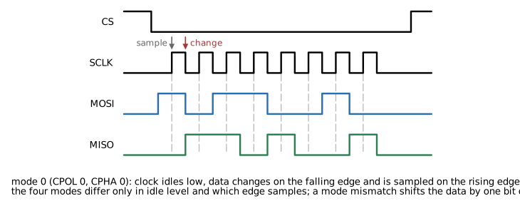 Figure 3. SPI mode 0 timing. Data changes on the falling clock edge and is sampled on the rising edge; the four modes differ in idle level and sampling edge.
SPI is a four-wire, push-pull, single-master synchronous bus: SCLK, MOSI, MISO, and a chip select per slave. Push-pull drivers give fast edges at any bus loading, the clock rate is limited by the slowest device and by signal integrity, and there is no acknowledgement, so a dead slave and a working one look the same until the data is examined.
Modes
CPOL sets the clock's idle level (0 low, 1 high); CPHA sets whether data is sampled on the first (0) or second (1) clock transition of each bit. The four combinations are modes 0 to 3. Most devices support one or two. A mode mismatch shifts data by half a clock, which reads as the data misaligned by one bit, or the first bit lost, or the last bit doubled. The device datasheet's timing diagram, not its mode number (which some vendors define differently), is the reference.
Clock rate and signal integrity
The maximum clock is the lower of the master's, the slave's, and what the wiring supports. Timing closure requires
for the read direction, where the slave's clock-to-output delay (often 10 to 30 ns) plus two propagation delays (out on SCLK, back on MISO) must fit in one clock period. At 25 MHz the period is 40 ns and a 30 ns slave delay leaves nothing for a cable. This round-trip limit is why long SPI links run slow regardless of the parts' ratings.
Above about 10 MHz, or with any trace longer than a few centimeters carrying a fast edge, the lines need signal integrity treatment: series termination resistors (22 to 47 Ω) at the driver to damp ringing, a ground return next to every signal on a cable or ribbon, and a clock that is not routed past the slaves' analog pins. SCLK is the critical signal: a ring on SCLK that crosses the threshold twice clocks an extra bit.
Multi-slave buses
Each slave needs its own chip select, held inactive during other slaves' transactions. MISO must tristate when the slave is deselected; a slave that does not (some cheap peripherals, and any slave whose CS is mis-wired) holds the line and corrupts every other device's reads. A resistor in series with a suspect MISO lets the bus work while it is identified. Daisy-chained SPI (MISO to the next MOSI) is a different topology used for shift-register style devices and requires all devices to support it.
Levels
Push-pull outputs into an input on a different voltage domain need a translator: a resistor divider for a unidirectional line at low speed, a dedicated direction-controlled translator IC otherwise. MISO from a 3.3 V slave into a 5 V master's input needs the input to recognize 3.3 V as high (most 5 V CMOS inputs need 3.5 V and do not); MOSI from a 5 V master into a 3.3 V slave needs the slave to be 5 V tolerant.
Bring-up
- Scope SCLK, CS, and MOSI at the slave with a known write (a register write followed by a read-back). Confirm the idle level, the edge polarity against the datasheet timing diagram, and the clock rate.
- Confirm CS is asserted before the first clock and released after the last, with the datasheet's setup and hold margins.
- Read a known register (device ID). If the value is shifted by one bit, the mode is wrong; if it is all ones or zeros, MISO is not driven (CS, power, or a stuck MISO from another slave); if it is right for one device and wrong for a second, the second's tristate or CS is at fault.
- Reduce the clock to 1 MHz if anything is marginal; if the fault disappears, it is signal integrity or timing closure, not protocol.
UART
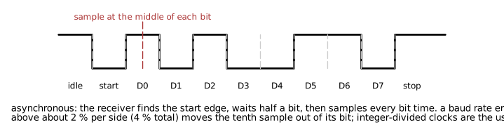 Figure 4. A UART frame: idle high, one start bit, eight data bits least-significant first, one stop bit. The receiver samples at the middle of each bit time from the start edge.
A UART sends bytes asynchronously: the receiver detects the falling start edge, waits half a bit period, and samples every bit period after. There is no clock line; each end's baud clock must match within the tolerance that keeps the tenth sample inside its bit.
Baud rate error
With 10 bits per frame and sampling at mid-bit, the accumulated timing error at the last bit must be under half a bit: 5 % total between both ends, and the usual allocation is 2 to 3 % per side after allowing for edge distortion. A UART clocked from a divided system clock produces a baud rate that may be several percent off: 8 MHz / 115200 = 69.4, so the divider is 69 and the rate is 115942, 0.6 % high, which is fine, but 8 MHz at 921600 is 8.7 divided to 9, a 3.5 % error, which is not. Crystals of 11.0592, 14.7456, and 18.432 MHz exist because they divide to standard baud rates exactly; modern UARTs with fractional dividers make this less of an issue but the check is still made.
Levels and polarity
Logic-level UART is push-pull, idle high, at the device's supply voltage; connecting two devices means matching voltage domains (or a translator) and crossing TX to RX. RS-232 inverts the logic and uses ±3 to ±15 V through a transceiver; connecting a logic-level UART directly to an RS-232 port produces garbage or damage. Some modules use inverted logic-level UART, and some radios expect a specific idle level; the datasheet's waveform is the reference.
Flow control
Hardware flow control (RTS/CTS) is needed whenever the receiver cannot keep up with a continuous stream, which for a microcontroller at 1 Mbaud with a 16-byte FIFO is common. Without it the symptom is dropped bytes under load, not on the bench.
Bring-up
- Scope TX at the transmitter: confirm the idle level, the bit period against the intended baud rate (measure it; do not trust the divider), and the frame format (8N1 is the default and not universal).
- Loop TX to RX on one device to test its own UART before involving the other end.
- If the receiver sees garbage: baud rate, then polarity, then frame format, then levels. Garbage that is consistent (the same wrong byte for the same sent byte) is a baud or format mismatch; garbage that varies is a level or noise problem.
- Under sustained traffic, count received against sent; a shortfall is flow control or interrupt latency.
RS-485
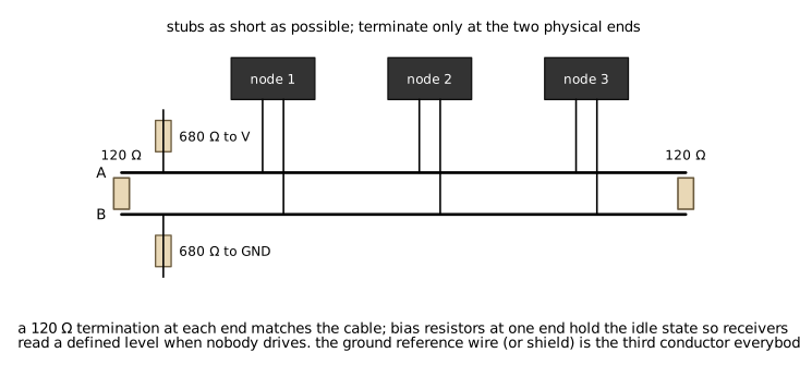 Figure 5. An RS-485 bus: two-wire, terminated at both physical ends with 120 Ω, biased at one end, with short stubs to each node.
RS-485 is a differential, half-duplex (two-wire) or full-duplex (four-wire), multi-drop bus for distances to 1200 m and rates to tens of megabits. The transceiver drives a differential voltage of at least 1.5 V into the terminated bus; the receiver detects the polarity of a difference above 200 mV. The common-mode range is -7 to +12 V, which is the allowed ground potential difference between nodes plus the driver's own offset.
Termination
The bus is a transmission line, typically 120 Ω twisted pair, and is terminated with 120 Ω at each of its two physical ends and nowhere else. Consequences:
- No termination: reflections at the open ends corrupt bits on any bus longer than a few meters at moderate rates.
- Termination at every node: the parallel load exceeds the driver's capability (32 unit loads, or fewer at 60 Ω), the differential swing collapses, and the bus fails once enough nodes are present.
- Termination at a node that is not at the end, with the bus continuing past it: the unterminated tail reflects.
Stubs from the bus to each node should be short (under a tenth of the rise time's electrical length; a few centimeters at 1 Mbps, a meter at 100 kbps). A star topology is a set of long stubs and works only at low rates or with a repeater per branch.
Biasing
When no driver is active the bus floats, the terminations pull the difference to zero, and the receiver output is undefined; a receiver without fail-safe biasing then produces noise as data. A bias network at one end (a pull-up on A and a pull-down on B, typically 680 Ω each at 5 V with 120 Ω terminations) holds the idle difference above 200 mV. Many modern transceivers include a fail-safe receiver that reads an open or shorted bus as idle and need no external bias; the datasheet says which.
Ground
RS-485 is differential but not isolated: the common-mode range is only -7 to +12 V, and two nodes on separate mains grounds can differ by more than that. A third conductor carrying signal ground between nodes, connected through a 100 Ω resistor at each node to limit the loop current, keeps the common mode in range. Long runs between buildings, or nodes on different mains phases, need isolated transceivers, which raise the common-mode tolerance to the isolation rating.
Direction control
A half-duplex transceiver's driver enable must be asserted before the first bit and released after the last stop bit, typically from a UART's TX-enable output or a timer. Releasing early truncates the last byte; releasing late holds the bus and blocks the reply. Transceivers with automatic direction control (driving only during the low bits) avoid the timing but need the bias network for the high bits.
Bring-up
- With the bus idle, measure A minus B at a receiver: it should be above 200 mV (biased) or the transceiver should be fail-safe.
- With a node transmitting, scope A and B at the far end: a clean differential swing of 1.5 V or more, no ringing, no slow edges. Ringing means a missing termination; a small swing means too many terminations or a shorted pair.
- Measure the common-mode voltage between the nodes' grounds. Above a few volts, add or repair the ground wire, or isolate.
- Check the driver enable timing on the scope relative to the data.
- Test at the longest cable, the lowest supply, and with every node connected.
CAN
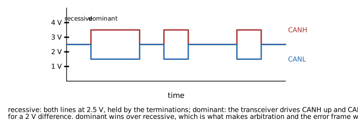 Figure 6. CAN bus levels. Recessive is both lines at 2.5 V; dominant is CANH driven up and CANL driven down. Dominant overrides recessive, which is what arbitration relies on.
CAN is a differential, two-wire, multi-master bus with hardware arbitration and error handling, at rates to 1 Mbps (classic) or 5 to 8 Mbps data phase (CAN FD). The transceiver drives a dominant state (CANH about 3.5 V, CANL about 1.5 V) and releases to a recessive state (both about 2.5 V, held by the terminations). Dominant overrides recessive, so when two nodes transmit at once the one sending a dominant bit wins arbitration and the other backs off.
Termination
120 Ω at each of the two ends of the bus, and nowhere else, as for RS-485. A bus with one termination works on the bench at low rates and fails with length or speed; with none it usually does not work at all. Split termination (two 60 Ω with the center tapped to ground through 4.7 nF) improves common-mode noise and emissions and is common in automotive designs. Stubs are limited to about 0.3 m at 1 Mbps.
Bit timing
CAN's bit rate is set by a bit timing configuration (prescaler, time segments, sample point) that must be compatible across all nodes; two nodes at "500 kbps" with different sample points and clock tolerances may not communicate. The sample point should be at 75 to 87.5 % of the bit; the oscillator tolerance requirement is tight (±0.5 % at 1 Mbps with a long bus), which rules out RC oscillators. A CAN node that transmits with no other node to acknowledge goes into error-passive state and retries indefinitely; a two-node bench test needs both nodes running.
Ground
Like RS-485, CAN transceivers tolerate a limited common-mode range (typically -2 to +7 V, more for automotive parts) and need a common ground reference. The vehicle chassis provides it in a car; a multi-drop industrial bus needs a ground conductor or isolated transceivers.
Bring-up
- With the bus idle, both lines should sit at about 2.5 V and the differential at zero; 60 Ω between CANH and CANL with power off confirms two terminations.
- With a node transmitting, scope CANH and CANL: dominant differential of about 2 V, clean edges, and the recessive return to 2.5 V without ringing.
- If a node reports errors: bit timing configuration (compare the sample points), the transceiver's standby pin, and whether a second node is present to ACK.
- A CAN analyzer on the bus shows error frames, which identify which node is transmitting badly.
Level translation
| Situation | Solution | Notes |
|---|---|---|
| Push-pull output at a higher voltage into a lower-voltage input | Resistor divider (slow), or a translator IC | A divider's output impedance limits speed to a few megahertz |
| Push-pull output at a lower voltage into a higher-voltage input | Check VIH: many 5 V inputs accept 3.3 V (TTL thresholds at 2 V), CMOS inputs do not | A translator IC or a 5 V-tolerant part |
| Open-drain bus across domains (I2C) | Single MOSFET per line, or a bidirectional open-drain translator | Pull-ups on both sides |
| Bidirectional push-pull (SPI MISO from several domains) | Direction-controlled translator, or auto-sensing translator IC | Auto-sensing translators have weak drive and limited speed |
| Isolated bus | Digital isolator with the interface's transceiver on the far side | Powered from an isolated supply |
An input with a higher voltage than its supply pin, on a device without tolerant inputs, forward-biases the protection diode into the supply. The symptom is a device that powers itself through its input when its supply is off, latch-up, or a slow failure.
Diagnostic method
For any bus that does not work:
- Power and reset at every device on the bus, at the device's pins.
- Levels at the pins, on a scope with a short ground: idle level, driven level, and whether they meet the receiver's thresholds with margin.
- Edges: rise and fall times against the bus's limits, ringing, and glitches on any clock line.
- Timing: the clock rate, setup and hold at the receiver, and for asynchronous buses the bit period.
- Protocol: only after the electrical layer is clean, use a logic analyzer or bus analyzer to read the transactions.
- Change one variable: clock rate, cable length, pull-up value, or node count, and watch which one moves the failure.
A fault that appears only with the long cable, only at temperature, or only with all nodes present is electrical. A fault that is the same on the bench with a 10 cm jumper is protocol or configuration.
Design errors
- I2C pull-up too large for the bus capacitance. Correction: compute Rp,max from Cb and the mode; measure the rise time.
- I2C pull-up below the weakest device's sink capability. Correction: Rp,min from the weakest device's IOL.
- SPI clock at the device maximum over a cable. Correction: timing closure including propagation; series termination; reduce the clock.
- SPI slave that does not tristate MISO. Correction: a slave with a proper tristate, or a buffer gated by CS.
- UART baud from a non-dividing clock. Correction: a baud-friendly crystal or a fractional divider; measure the error.
- RS-485 terminated at every node or not at all. Correction: 120 Ω at the two ends only; bias at one end or fail-safe receivers.
- RS-485 or CAN with no ground reference between nodes. Correction: a ground conductor with current-limiting resistors, or isolation.
- CAN bit timing copied from another node with a different clock. Correction: recompute for the local clock and align the sample points.
- Voltage domains crossed without translation. Correction: check VIH, VIL, and input tolerance for every crossing; translate where needed.
- Bring-up done with a logic analyzer only. Correction: scope the edges and levels first.
Limitations of this document
- Timing numbers (rise time limits, sink currents, common-mode ranges) are from the I2C-bus specification, the RS-485 (TIA-485) and CAN (ISO 11898-2) standards as commonly implemented; the transceiver and device datasheets govern.
- SPI has no formal standard; every device's timing diagram is its own specification.
- Protocol-level behavior (I2C SMBus timeouts, CAN error counters and bus-off recovery, UART framing options) is covered only as it explains an electrical symptom.
- High-speed and long-distance variants (I3C, SPI above 50 MHz, CAN FD signal integrity above 2 Mbps) need treatment beyond this note.