Maxwell's Equations for Circuit Designers
noteThe four equations read as plain statements about fields; the integral, differential, phasor, potential, quasi-static, and lumped-circuit forms and what each view is good for; what follows from them (waves, impedance, energy flow, skin effect, inductance, capacitance); and the mental models a board designer actually uses: signals live in the dielectric, return current hugs the trace, every loop is an antenna, displacement current closes every circuit, and when a wire stops being a wire.
related tools: trace impedance, trace inductance, plane capacitance, rise time, bandwidth, and critical length, reflection coefficient
Scope: the four equations at the level needed to reason about circuits and printed circuit boards, not to solve them. Every field solver, every rule of thumb about return paths, decoupling, crosstalk, and emissions, and the whole of circuit theory follow from these four statements; the note makes the path from each equation to the bench explicit. Antenna theory, waveguides, and relativistic formulation are outside the scope.
Common errors
- A ground plane understood as a place where current disappears. Current returns on the plane, directly beneath the trace, in a strip a few trace heights wide, and it does so because of Faraday's law, not because the plane is labelled ground.
- Signals understood as electrons moving through copper. The signal is an electromagnetic field in the dielectric between the trace and its return; it moves at half the speed of light in FR-4. The electrons drift at millimeters per second and the copper only guides the field.
- Kirchhoff's laws treated as fundamental. They are the limit of Maxwell's equations when the circuit is small compared with a wavelength and no flux threads the loops. A 10 cm trace at 1 GHz breaks both assumptions, and so does a 10 cm loop next to a switching converter at 100 kHz.
- Inductance thought of as a property of a wire. Inductance belongs to a loop, the loop the current closes through. A trace has no inductance until its return path is known, and moving the return path changes it by orders of magnitude.
- Capacitance thought of as a property of a capacitor. Any two conductors at different potentials store charge; every pad, plane, and cable has it, and at high frequency the stray capacitance is the circuit.
- A slot in a plane treated as harmless because DC still flows around it. The high-frequency return current cannot go around; it is forced into a large loop, and the loop radiates and couples into everything crossing the slot.
- Decoupling capacitors placed by value rather than by loop. A capacitor's job is to close a current loop close to the load; its inductance, set by the loop through its pads and vias, decides its usefulness above a few MHz, and the value hardly matters there.
The quantities
| Symbol | Name | Unit | What it is |
|---|---|---|---|
| E | electric field | V/m | force per unit charge; the gradient of voltage in the static case |
| B | magnetic flux density | T (V·s/m²) | the field that pushes on moving charge and threads loops as flux |
| D | electric flux density | C/m² | E scaled by the material: D = εE |
| H | magnetic field | A/m | B scaled by the material: B = µH |
| ρ | charge density | C/m³ | where the charge is |
| J | current density | A/m² | where the charge is moving |
| ε, µ | permittivity, permeability | F/m, H/m | the medium; ε₀ = 8.85 pF/m, µ₀ = 1.257 µH/m; FR-4 has ε = 4.3 ε₀ and µ = µ₀ |
| Φ | flux | Wb or C | the field integrated over a surface: how much of it passes through |
Two constants of the medium fix everything that follows: the speed at which fields travel and the ratio of E to H in a travelling wave.
In vacuum v is 300 mm/ns and η is 377 Ω. In FR-4 v is about 145 mm/ns, which is 6.9 ps per millimeter, and η is 182 Ω.
The four equations
Each equation is given in integral form (a statement about a region) and differential form (a statement about a point), then read in words, then followed to the board.
Gauss's law for electric fields: charge makes electric field
Electric field lines start on positive charge and end on negative charge. Draw any closed surface: the net field leaving it equals the charge inside it. No charge inside, no net field leaving, so field lines that enter must leave.
What follows for the board:
- Capacitance. Put charge Q on a trace; field lines leave it and must end on negative charge somewhere, on the plane, the neighboring trace, the enclosure. The voltage that results per unit of charge is 1/C. Every conductor pair has a capacitance, and the closer and larger the conductors the bigger it is. Between a trace and a plane at height h, roughly ε times the trace area over h; between two planes, ε times the overlap over the gap, which is about 100 pF per square inch at 4 mil spacing.
- Shielding. Field lines cannot pass through a conductor, since the free charge in it rearranges until the field inside is zero. A grounded plane between two traces ends the field lines from one before they reach the other: that is what a shield does, and it works for electric fields at any frequency, including DC.
- Fringing. Field lines spread. A trace's capacitance to a plane is 20 to 50 percent more than the parallel-plate estimate because of the field at its edges, and the fringe field is the part that reaches the neighboring trace as capacitive crosstalk.
Gauss's law for magnetic fields: there is no magnetic charge
Magnetic field lines have no beginning and no end; they close on themselves. Whatever flux enters a closed surface leaves it.
What follows: magnetic field cannot be blocked the way electric field can. A conductor does not end a B field line. Magnetic shielding works either by giving the flux an easier path around the protected region (high-permeability material, which is heavy, expensive, and saturates) or, at high frequency, by inducing eddy currents in a conductor that produce an opposing field (which is Faraday's law, below, and needs the skin depth to be small). At 50 Hz a copper enclosure does nothing against a transformer's stray field; at 10 MHz it works well.
Faraday's law: a changing magnetic field makes a circulating electric field
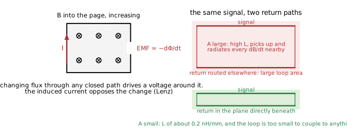 Figure 1. Faraday's law on a loop and on a board. A changing flux through any closed path drives a voltage around it. The same signal trace has a large loop area when its return is routed elsewhere and a tiny one when the return is the plane beneath it; the loop area sets the inductance, the pickup, and the radiation.
Take any closed path. The voltage around it equals the rate of change of magnetic flux through it, with a sign such that the induced current opposes the change. This is the equation that breaks Kirchhoff's voltage law: the voltages around a loop sum to zero only when no changing flux threads the loop. It is also the equation of every transformer, every inductor, every ground bounce, and every pickup problem.
What follows for the board:
- Inductance is loop area. A current I in a loop produces a flux Φ = LI through it; L is set by the loop's geometry, and for a wire above a plane by the area between them. Halve the height of a trace above its plane and the inductance per length halves. Route the return on the far side of the board and it increases tenfold.
- L di/dt is a real voltage. A ground path of 5 nH carrying a current edge of 1 A in 2 ns develops 2.5 V across it. Every chip that switches current through its ground pin bounces its ground by this amount, and every "noise" on a supply rail at a switching edge is this equation.
- Every loop is a receiving antenna. A 1 cm² loop in a 1 µT field changing at 1 MHz has 6 mV induced around it. Loop area is the pickup; twisting a pair or routing over a plane cancels it.
- Return current hugs the trace. The current chooses its return path to minimize the flux it produces, which is to say the loop area, which is to say the inductance. Above a few tens of kHz that path is directly beneath the trace, and it stays there unless a slot forces it away.
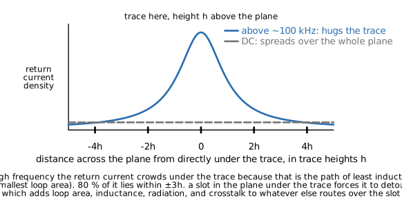 Figure 2. Return current density in a plane beneath a trace at height h. At DC the current spreads over the whole plane; above about 100 kHz it crowds under the trace, with 80 percent within three trace heights, because that is the path of least inductance.
Ampère's law with Maxwell's term: current, or a changing electric field, makes a circulating magnetic field
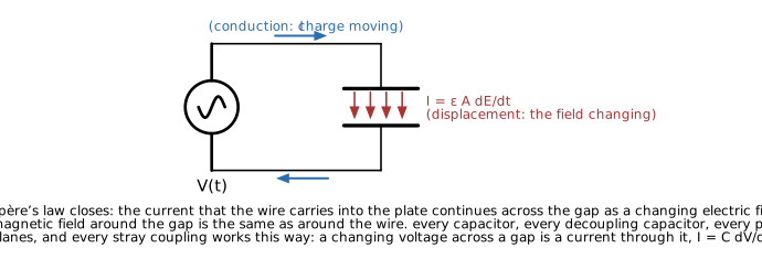 Figure 3. Displacement current. The conduction current in the wires continues across the capacitor gap as a changing electric field, and the magnetic field around the gap is the same as around the wire. Every capacitor, every plane pair, and every stray coupling carries current this way.
Take any closed path. The magnetic field circulating around it equals the current passing through it, plus the rate of change of electric flux through it. The second term is Maxwell's addition, and it is the term that makes the equations produce waves. Its reading for a circuit designer is direct: a changing electric field is a current. It carries the current across a capacitor's gap, and it is the reason a circuit that is "open" at DC conducts at high frequency through every stray capacitance.
What follows for the board:
- Current always closes. There is no such thing as a current that goes somewhere and stops. It returns, through copper or through displacement current in a dielectric, and the designer's job is to know which and where.
- Decoupling is a displacement-current path. A switching output draws a current pulse; it must return to the supply through the shortest loop, which is the nearest capacitor's displacement current, then the plane pair's displacement current, then the bulk capacitor, then the regulator. Each stage has a loop, and each loop's inductance sets how fast that stage can supply current: a 0402 capacitor with 1 nH of mounting inductance is useless above a few hundred MHz, where the plane pair takes over.
- Magnetic field surrounds every current, including the displacement current in a capacitor and the return current in a plane. The H field of a trace and its return, being equal and opposite and close together, cancels at any distance large compared with their spacing: the far field of a well-routed signal is small.
- Crosstalk has two halves. A changing current in one trace produces a changing B that threads the neighbor's loop (Faraday: inductive crosstalk); a changing voltage on one trace produces a changing E that ends on the neighbor (Gauss and Ampère: capacitive crosstalk). Both fall with spacing and with height above the plane, and both are the same physics as the signal itself.
The forms, and what each view provides
The equations are written in several forms. They are the same physics; each form makes a different question easy.
Integral form
Statements about regions: the flux through a surface, the circulation around a path. This is the form for reasoning. Draw the loop, draw the surface, ask what threads it. Almost every rule of thumb about boards is an integral-form argument: loop area, enclosed current, charge on a conductor. It is also the form in which the laws are measured, since a probe measures the voltage around a loop, not a curl at a point.
Differential form
Statements about points: divergence and curl. This is the form for computation and for deriving consequences. Field solvers discretize the differential form; the wave equation, the skin depth, and the transmission-line equations are derived from it. The designer rarely uses it directly, but knows that the solver's answer and the loop argument agree because they are one set of equations.
Time domain and frequency domain
Replace every d/dt with jω and every field with a phasor. The equations become algebraic, materials with loss become complex permittivity and permeability, and the concept of impedance appears: for a sinusoid, the ratio of E to H in a wave, or of V to I on a line, is a fixed complex number. The frequency-domain view gives the S-parameter, the Bode plot, the impedance of a decoupling network against frequency, and the meaning of "the plane pair is capacitive below 200 MHz and inductive above". The time-domain view gives the reflection on a TDR trace and the ground-bounce transient. A fast edge contains frequencies up to about 0.35 divided by its rise time, so a 1 ns edge is a 350 MHz problem in the frequency domain, and both views must be held at once.
Constitutive relations and materials
D = εE and B = µH are where the material enters. In the dielectric of a board, ε sets the propagation speed and the capacitance per length; its loss tangent sets the attenuation. In a ferrite bead, µ is large and lossy in a chosen band, which is what turns it into a frequency-dependent resistor. In copper, conductivity σ makes J = σE, and it is this relation together with Faraday and Ampère that produces the skin effect.
Potentials
E and B can be written in terms of a scalar potential V and a vector potential A:
This is the form in which circuit theory is born. Voltage is the scalar potential, and it is only well defined, as a number that a node has, when the second term is negligible: when no changing flux threads the region. When it is not negligible, "the voltage between two points" depends on the path taken between them, which is what a probe ground lead demonstrates when it picks up a switching converter's field. The vector potential is the term behind inductance: the EMF a changing current induces in a loop is the loop integral of dA/dt.
Quasi-static approximations
When the structure is small compared with a wavelength, the coupling between Faraday and Ampère that produces waves can be dropped, and the fields are found as if the source were static and then allowed to vary.
- Electro-quasi-static (EQS): the electric field dominates; capacitance, high-impedance nodes, electrostatic discharge, sensor front ends.
- Magneto-quasi-static (MQS): the magnetic field dominates; inductors, transformers, motors, current loops, eddy currents, skin effect.
Most of a board at most frequencies is one or the other, and the designer's first question about a node is which one: a high-impedance node is EQS and fears capacitive coupling and leakage; a low-impedance, high-current path is MQS and fears loop area and mutual inductance.
The lumped-circuit limit
Kirchhoff's laws are the quasi-static equations with one more approximation: that every element is small enough, and every loop encloses little enough flux, that the fields can be assigned entirely to the elements. Then charge conservation gives KCL, Faraday with no stray flux gives KVL, and the fields are hidden inside the symbols R, L, and C. The approximation holds when the largest dimension of the circuit is under about a tenth of a wavelength at the highest frequency present, and when no unintended loop encloses a changing flux. In FR-4 at 1 GHz a tenth of a wavelength is 15 mm; a 1 ns edge sees 350 MHz, so a trace over about 40 mm is a transmission line, not a wire.
| Frequency | Wavelength in FR-4 | λ/10 | A 10 cm trace is |
|---|---|---|---|
| 1 MHz | 145 m | 14.5 m | a wire |
| 10 MHz | 14.5 m | 1.45 m | a wire |
| 100 MHz | 1.45 m | 145 mm | on the edge |
| 300 MHz (a 1 ns edge) | 480 mm | 48 mm | a transmission line |
| 1 GHz | 145 mm | 14.5 mm | a transmission line, three wavelengths of it at 5 GHz |
What follows from the equations
Waves and the speed of the signal
Faraday's curl of E feeds Ampère's curl of H and back. Combined, they give a wave equation whose solutions travel at v = 1/√(µε). On a board the signal is exactly such a wave, guided by the trace and its return: an E field between the two conductors and an H field around the current, moving along the line together.
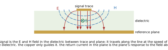 Figure 4. The fields of a signal on a trace over a plane. E runs from trace to plane, H loops around the trace, and the energy flows along the dielectric in the direction of E × H. The copper carries the current that the field at its surface requires; the signal itself is in the dielectric.
Consequences: propagation delay is about 7 ps per millimeter in FR-4, a signal and its return travel together so the return must be continuous the whole way, and the dielectric, not the copper, sets the speed, so a trace on the outer layer (half its field in air) is faster than the same trace buried.
Characteristic impedance
The ratio of the wave's voltage to its current is fixed by the geometry and the material: Z₀ = √(L/C) per length, which for a trace over a plane depends on width, height, and ε. Where Z₀ changes, part of the wave reflects, in the proportion (Z₂ − Z₁)/(Z₂ + Z₁). Every via, every neck-down, every gap in the return plane is a Z₀ change and therefore a reflection. Terminating a line in its Z₀ absorbs the wave with no reflection; this is the whole of the matching problem, and the tools page has calculators for Z₀ and for reflections.
Energy flows in the fields
The Poynting vector S = E × H is the power flow per unit area, and it points along the dielectric between the conductors, not along the copper. A resistor's power arrives through the field around it, and a power supply's energy reaches the load through the space between the supply traces. The practical reading: the region between a trace and its return is where the signal is, and anything placed in that region (a slot, another trace, a change in dielectric) changes the signal. The copper is a boundary condition.
Skin effect
Inside a conductor, Faraday and Ampère together give a diffusion equation: a changing field penetrates a conductor only to a depth
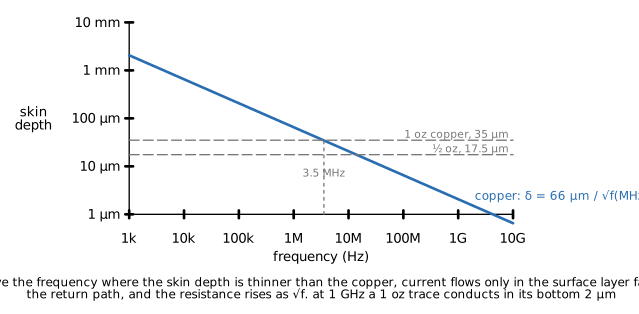 Figure 5. Skin depth in copper against frequency. Above about 3.5 MHz the depth is less than 1 oz copper, current flows only in the surface facing the return path, and the resistance rises as the square root of frequency.
Above a few MHz a trace's current flows in its bottom few micrometers, on the face toward the plane, and a plane's return current flows in its top few micrometers. Resistance rises as √f, which is why long high-speed lines lose their high-frequency content and edges slow. Skin effect is also why a thick ground plane does not help at high frequency, why the inside of a shield carries no current, and why litz wire exists.
Inductance and capacitance, properly
Inductance is magnetic energy per unit current squared: the flux through the loop the current closes. Capacitance is electric energy per unit voltage squared: the charge the conductors hold at a given voltage. Neither is a property of one conductor. Both are properties of a geometry, and both change when the geometry changes: moving a trace closer to its plane lowers L and raises C in the same proportion, which is why Z₀ falls and the delay does not change.
Mental models for the board
The equations are used on a board as a short list of habits.
- Find the return path first. Every signal, every power pulse, every clock has a return current, and Faraday's law puts it directly beneath the outgoing path at any frequency that matters. Before routing a trace, know which plane returns it, and keep that plane continuous under the whole route. A layer change is a return-path change and needs a return via or a decoupling capacitor between the two planes next to the signal via.
- Loop area is the enemy. Inductance, pickup, ground bounce, and radiation all scale with the area between a current and its return. Shrink it: closer planes, shorter leads, decoupling capacitors beside the pin, no slots. The E field of a small loop cancels; the H field of a small loop cancels; a small loop is quiet in both directions.
- Current closes through capacitance when it cannot close through copper. Where a return plane is missing, the current still returns, through whatever displacement path is available, and that path is large, uncontrolled, and radiates. Slots, split planes, and connectors without enough ground pins all force this.
- Every node has an impedance to its surroundings. A high-impedance node couples through its stray capacitance (EQS): guard it, keep it small, keep switching nodes away. A low-impedance high-current path couples through mutual inductance (MQS): keep its loop small and keep sensitive loops out of its field.
- The dielectric between a trace and its plane is the signal. Do not route anything through it, do not change it mid-route, and do not let another trace's field share it. Crosstalk is field sharing; spacing traces by three times their height above the plane reduces it to a few percent.
- Fast edges are high frequencies. An edge's spectrum reaches about 0.35 divided by the rise time. A 1 ns edge is a 350 MHz signal for purposes of return paths, decoupling, and radiation, regardless of the clock rate. Slowing edges that need not be fast is the cheapest EMC measure there is.
- Impedance changes reflect. A via, a stub, a connector, a change of layer, a neck under a component: each reflects part of the wave. Above the lumped limit, the trace is a component with a value, Z₀, that must be kept constant and terminated.
- Skin depth sets where the current is. Plating, surface roughness, and the face of the conductor toward the return matter at high frequency; thickness beyond two skin depths does not.
- Voltage is well defined only where flux is not changing. A probe ground lead of 10 cm closes a loop of tens of square centimeters; near a switching converter the "measurement" is the flux through that loop. The Oscilloscope Probing note covers the remedies. The same fact means that "ground" is a single potential only at DC; at 100 MHz two points on a plane 5 cm apart differ by whatever L di/dt flows between them.
- When the lumped model is wrong, it is wrong quietly. A circuit that violates the lumped limit does not refuse to simulate; the simulation is simply of a different circuit than the board. The check is dimension against λ/10 and loop area against dB/dt.
Worked numbers
- Ground bounce. A QFN's ground bond and via, 2 nH, with 16 outputs switching 20 mA each in 1 ns: di/dt = 0.32 A/ns, V = 2 nH × 0.32 A/ns = 0.64 V of bounce.
- Decoupling reach. A 100 nF capacitor with 1 nH of mounting loop resonates at 16 MHz; above that it is an inductor, and at 300 MHz its impedance is 1.9 Ω. Ten of them in parallel are 0.19 Ω. A plane pair of 100 cm² at 4 mil spacing is 1.6 nF with near-zero inductance and takes over above a few hundred MHz.
- Loop pickup. A 4 cm² loop 2 cm from a trace carrying 1 A switching in 10 ns: B at 2 cm is about 10 µT, dB/dt is 1 mT/µs, EMF is 4 cm² × 1 mT/µs = 0.4 V.
- Trace delay. 150 mm of stripline in FR-4: 150 × 6.9 ps = 1.0 ns, comparable to the rise time of the signal, so the far end must be treated as a transmission line.
- Return-path spread. A trace 0.2 mm above its plane: 80 percent of its return current lies within 0.6 mm either side. A slot 1 mm from the trace is out of the way; a slot under the trace is a discontinuity.
- Skin depth at 100 MHz. 6.6 µm; a 35 µm trace conducts in 19 percent of its thickness on one face. Its AC resistance is about five times its DC resistance.
Design errors
- A signal routed across a split plane, the return forced around the split, with emissions at the signal's harmonics and crosstalk into every other trace crossing the split.
- A high-current loop routed wide and open through a converter, with 100 nH of loop inductance ringing at every switching edge.
- A decoupling capacitor 10 mm from its pin, adding 8 nH to the loop and doing nothing above 50 MHz.
- A 20 cm cable with a single-ended signal and no return next to it, the loop closed through the chassis and the whole thing radiating.
- A probe ground clip 15 cm long on a switching node, measuring the flux through the clip loop and reporting it as ringing.
- An analog input trace routed under a switching inductor, in the inductor's fringe field, with the switching frequency in every reading.
- A trace treated as a wire at 200 MHz because the clock is only 20 MHz, ignoring the edge's spectrum.
- Copper thickened to cure high-frequency loss, which lives in the top few micrometers and in the dielectric.
Limitations of this document
The equations are stated and read, not solved; field solvers, transmission-line theory, and antenna theory build on them and are not covered here. Material behavior (magnetic saturation, dielectric dispersion, the frequency dependence of loss tangent) is mentioned only where it changes a rule. The PCB Layout, Ground Planes, PCB Stackup, Oscilloscope Probing, and EMC notes apply these models in detail; this note is the reason those notes say what they say.