God-Mode Circuit Analysis
noteReading a circuit by inspection instead of by equation: the order of operations, DC first, the frequency map, impedance numbers worth memorizing, Thevenin and Norton, superposition and half circuits, op-amps and transistors by inspection, Bode sketching, time-domain estimates, the sanity checks that catch most mistakes, worked examples, and drills to make it automatic.
related tools: voltage divider, rc charge time, opamp gain stage, low pass filter (RC), high pass filter (RC), reactance and lc resonance
Scope: a method for understanding a circuit quickly and approximately, in the head, before or instead of simulating it. The goal is 10 to 20 % accuracy in under a minute, with the structure of the answer correct: which parts matter, which do not, what sets each voltage and current, and how the picture changes with frequency. Exact analysis is for after the picture is right. The techniques are standard; the value is in the order they are applied and in the numbers kept in memory so that no arithmetic interrupts the reading.
Order of operations
Every circuit is read the same way. Skipping a step is how a wrong answer arrives with confidence.
| Step | Question | Tool |
|---|---|---|
| 1 | What is this? Where is the signal, the supply, the reference, the feedback? | Redraw, name the nodes |
| 2 | Where does everything sit at DC? | Capacitors open, inductors shorted, DC sources on, ideal-element rules |
| 3 | What are the corner frequencies, in order? | One RC or L/R product per reactive part, sorted |
| 4 | What does the circuit look like in each frequency band? | Capacitors and inductors replaced by opens and shorts band by band |
| 5 | What is the small-signal gain and impedance in the band of interest? | DC sources killed, dividers, Thevenin, op-amp and transistor rules |
| 6 | Is the answer possible? | Limits, power, sign, units, the remove-the-part test |
Steps 2 to 4 are the mental simulator: a DC operating point, then an AC sweep taken one decade at a time. Step 5 is where the equations would start on paper; by inspection it is usually a ratio of two resistances. Step 6 is not optional.
Reading the schematic
The first pass identifies structure, not values.
- Find the reference. Ground is a node, not a sink. Every current that leaves a source returns to it, and the path it takes back is part of the circuit whether or not it is drawn.
- Find the sources: supply rails, signal inputs, references. Mark which are DC (they will be shorted for AC analysis) and which carry signal.
- Trace the signal path from input to output and name every node on it. Three to six names is typical. A node with no name is a node that will be forgotten.
- Find the feedback path, if any: does the output reach an input? For an op-amp, which input? Count inversions around the loop; an odd count with the loop closed on the inverting input is negative feedback.
- Classify each capacitor by position. In series with the signal path it is a coupling capacitor and forms a high-pass with whatever resistance it drives. From a node to the reference it is a bypass or filter capacitor and forms a low-pass with whatever resistance feeds the node. Across a gain element from output to input it is compensation or a Miller capacitor. Across a supply it is decoupling.
- Classify each inductor the same way: in series it blocks high frequency, in shunt it blocks DC.
- Redraw if the drawing fights the reading. Supplies at the top, ground at the bottom, signal left to right, feedback above or below the forward path. A schematic drawn for layout convenience hides its own function.
A working habit: before any number, state in one sentence what the circuit is for. "A gain of about ten with a low-frequency cutoff near 20 Hz driving an ADC" is a hypothesis that every later step either confirms or refutes.
DC analysis
DC comes first because everything else is a small change around it. Transistor gains, diode resistances, and op-amp swing limits all depend on the operating point.
Rules for the DC picture:
- Every capacitor is an open circuit. Remove it from the drawing.
- Every inductor is a short circuit. Replace it with a wire (its winding resistance stays if it is more than a few percent of what is in series with it).
- A diode that is forward biased drops about 0.6 to 0.7 V for silicon, 0.2 to 0.4 V for Schottky, 1.8 to 3.3 V for LEDs by color. A diode that is reverse biased is an open. If the direction is not obvious, assume one, solve, and check for contradiction.
- A bipolar transistor in its active region has V, collector current equal to emitter current, and a base current small enough to ignore on a first pass. The question that sets everything is what sets the emitter current; usually it is an emitter resistor and a base voltage.
- A MOSFET in saturation has a gate-source voltage a few hundred millivolts above threshold. Its current is set by the source resistor and the gate voltage, or by the load if it is a switch.
- An op-amp with negative feedback holds its inputs at the same voltage and draws no input current. The output is at whatever voltage makes that true, provided that voltage is inside the supply.
With those substitutions most circuits become resistor networks with a few fixed drops, and the operating point is a divider calculation. Write the DC voltage beside every named node. Those numbers are needed twice more: to check that nothing is saturated or cut off, and to get the small-signal parameters of the transistors.
Loaded dividers are the common trap. A divider of over from a supply, feeding a load , delivers not but that value with replaced by . The Thevenin section makes this mechanical.
The frequency map
A circuit with reactive parts is not one circuit. It is a sequence of resistive circuits, one per frequency band, and the boundaries between the bands are the corner frequencies. Building the map is the single most productive step in the whole method.
For each capacitor, find the resistance it works against and compute the corner:
The resistance is the Thevenin resistance seen from the capacitor's terminals with all other capacitors treated as they are in the band being considered (open below their own corners, shorted above). On a first pass, take the nearest resistor in series or parallel and accept the error.
For each inductor:
Sort the corners. Below the lowest corner every capacitor is open and every inductor is a short: the DC picture. Above the highest corner every capacitor is a short and every inductor is open. Between two adjacent corners, the parts below their corner have switched and the parts above have not. Each band is a plain resistive circuit that can be read by inspection.
Two corners within a factor of three of each other interact and the response between them is rounded rather than cornered; the map still gives the right slopes on either side.
The map also says what each capacitor is for. A coupling capacitor whose corner is at 20 Hz is doing its job; the same capacitor with a corner at 2 kHz is eating the signal. A bypass capacitor whose corner is above the frequency it is supposed to remove is decorative.
Impedance by inspection
The map is only as fast as the arithmetic behind it. Two numbers make the arithmetic disappear.
The reactance of a capacitor is
so 1 µF at 1 kHz is 159 Ω, 100 nF at 1 kHz is 1.59 kΩ, 100 nF at 1 MHz is 1.59 Ω, and 10 pF at 100 MHz is 159 Ω. Any capacitor at any frequency is 159 Ω scaled by powers of ten.
The reactance of an inductor is
so 1 mH at 1 kHz is 6.28 Ω, 10 µH at 1 MHz is 62.8 Ω, and 10 nH at 1 GHz is 62.8 Ω.
The corner frequency of an RC pair follows from the same number: Hz for 1 kΩ and 1 µF, scaled by powers of ten in either part. 10 kΩ and 100 nF is also 159 Hz. 1 kΩ and 1 nF is 159 kHz.
| Pair | Corner |
|---|---|
| 1 kΩ, 1 µF | 159 Hz |
| 10 kΩ, 1 µF | 15.9 Hz |
| 1 kΩ, 100 nF | 1.59 kHz |
| 1 kΩ, 10 nF | 15.9 kHz |
| 1 kΩ, 1 nF | 159 kHz |
| 50 Ω, 10 pF | 318 MHz |
| 1 mH, 100 Ω | 15.9 kHz |
| 10 µH, 10 Ω | 159 kHz |
| 10 nH, 10 Ω | 159 MHz |
An LC pair resonates at
with characteristic impedance . 1 µH and 1 µF give 159 kHz and 1 Ω; 10 nH and 100 nF give 5 MHz and 0.32 Ω. At resonance a series LC is a short and a parallel LC is an open, and the parts see a voltage or current times what the source supplies, where for a series circuit and for a parallel one.
Parasitics are read the same way. A capacitor has 1 to 2 nH of lead and body inductance, so a 100 nF part resonates near 12 to 16 MHz and is an inductor above that. A resistor has about 0.2 pF across it and its leads add nanohenries. A trace has about 1 nH per millimeter and a via about 1 nH. Whether a parasitic matters is decided by comparing its reactance at the frequency of interest against the impedance around it; 1 nH is 6 Ω at 1 GHz and nothing at 1 kHz.
Reduction tools
Series and parallel combination, done approximately, removes most parts from the picture.
- Series: the larger dominates. 10 kΩ in series with 1 kΩ is 11 kΩ; call it 10 kΩ if 10 % is acceptable.
- Parallel: the smaller dominates. 10 kΩ in parallel with 1 kΩ is 909 Ω; call it 1 kΩ.
- Equal in parallel: half. Equal in series: double. Two parts in a 2:1 ratio in parallel give two thirds of the smaller.
- The 10:1 rule: any part more than ten times its neighbor in series (smaller) or in parallel (larger) can be dropped with less than 10 % error. Most circuits are designed with such ratios on purpose so that one part sets each quantity. Finding that part is the analysis.
The voltage divider is the unit of analysis. Output over input is , which is 1/2 for equal parts, about when is much larger, and about 1 when is much larger. Impedances divide the same way, so an RC low-pass at its corner is a divider of over , giving rather than because the two are at right angles.
The current divider is its dual. Current splits in inverse proportion to resistance: the branch with one tenth the resistance takes ten elevenths of the current.
Series and parallel impedances at a single frequency combine as magnitudes only when they are of the same kind. A resistor in series with a reactance gives , which is within 10 % of the larger whenever the ratio exceeds 2:1. Below that ratio, use for the equal case and interpolate.
Thevenin and Norton
Any two-terminal network of sources and linear parts is equivalent, as seen from those terminals, to one voltage source in series with one resistance (Thevenin) or one current source in parallel with the same resistance (Norton). The equivalent is what a load connected there sees, and it is the tool for every question of the form "what happens when this drives that".
The procedure:
- Open-circuit voltage : the voltage at the terminals with nothing connected.
- Equivalent resistance : replace every independent voltage source with a short and every independent current source with an open, then find the resistance looking into the terminals. Dependent sources stay; if there are any, apply a test source instead.
- Norton current , the current that would flow into a short across the terminals.
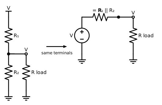 Figure 1. A loaded divider and its Thevenin equivalent. Looking back into the divider from the load, the supply is a short, so the two resistors are in parallel; the open-circuit voltage is the unloaded divider ratio.
For a divider of from a supply and to ground, and . This is worth memorizing outright; it answers the loaded-divider question, the base-bias question, the sensor-into-ADC question, and the reference-driving-a-comparator question in one line each.
Source transformation is the same equivalence used as a move. A voltage source in series with can be redrawn as a current source in parallel with , and back. Converting sources back and forth lets series parts be combined with parallel parts until one source and one resistance remain.
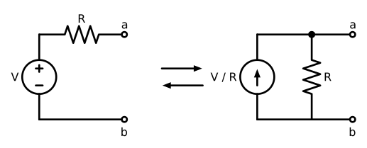 Figure 2. Source transformation. The two networks are indistinguishable from the terminals: the same open-circuit voltage, the same short-circuit current, the same resistance.
Reading impedance into a node is the Thevenin idea without the source. The resistance seen from a node is the parallel combination of every path from that node to a fixed voltage, with DC supplies counted as ground. A node with a 10 kΩ pull-up and a 1 kΩ pull-down has an impedance of about 900 Ω, and anything driving it works against that. An op-amp output looks like a few ohms; an op-amp input like an open; a transistor emitter like plus the base resistance divided by ; a collector or drain like the load resistor.
Thevenin resistance is also the resistance that sets a corner frequency. The capacitor on a node sees of that node, not any one resistor. A 100 nF capacitor on the 900 Ω node above has a corner at 1.8 kHz, not at 159 Hz or 15.9 kHz.
Superposition and half circuits
With more than one source, take them one at a time: keep one source active, replace every other voltage source with a short and every other current source with an open, solve, and add the results. Superposition holds for any linear circuit and is the natural way to read a circuit with a signal and a bias, or a differential and a common-mode input, or a supply ripple and a signal. It does not apply to power, which is quadratic, and it does not apply once a nonlinear part is in play; linearize first.
A differential pair, an instrumentation front end, or any symmetric circuit is read as two half circuits. For a differential input the axis of symmetry is at AC ground and each half is analyzed alone with half the input; for a common-mode input the axis carries no current and any part crossing it is either opened (if it crossed at a single point) or doubled (if it was shared, such as a tail resistor, which each half sees as twice its value). The two answers, differential gain and common-mode gain, come from two simple circuits instead of one difficult one.
AC small-signal analysis
Small-signal analysis is the DC picture inverted: every DC source becomes a short (voltage) or an open (current), every capacitor and inductor takes its impedance at the frequency of interest or its band substitute, and every nonlinear part becomes the linear model that fits its operating point. What remains is a linear network and the reduction tools apply.
Two rules make the band substitution fast:
- A capacitor whose reactance is less than a tenth of the resistance around it is a short. A coupling capacitor above its corner disappears; a bypass capacitor above its corner grounds its node.
- An inductor whose reactance is more than ten times the resistance around it is an open.
Gains by inspection are ratios of resistances. The general form for any single stage is
which reads as for a common-emitter stage with an emitter resistor, for an inverting op-amp, for a common-source stage, and when there is no source resistor. The sign is set by the topology; the magnitude is the ratio. Non-inverting forms are the same ratio.
Input impedance is what the source sees; output impedance is what the load sees. Each is a Thevenin resistance at the corresponding node. Loading between stages is the product of a divider at each interface: a stage with 1 kΩ output impedance driving a stage with 10 kΩ input impedance loses 9 %, and the overall gain is the product of the stage gains times the product of the interface dividers.
Op-amps by inspection
With negative feedback and an output inside its limits, an ideal op-amp obeys two rules: the inputs are at the same voltage, and no current flows into either input. Every op-amp circuit is solved by writing what those two rules force at the inverting input.
- Inverting: the inverting input is held at the voltage of the non-inverting input, usually ground. The input resistor converts the input voltage to a current, none of it enters the op-amp, all of it flows through the feedback element, and the output is whatever voltage puts that current through the feedback element. Gain is , and the input impedance is .
- Non-inverting: the inverting input is held at the input voltage. The feedback divider must reproduce the input at its tap, so the output is the input times . Input impedance is the op-amp's own.
- Anything else: find which node is held where and which current has only one place to go.
The feedback element read band by band gives the circuit's frequency response without algebra. A capacitor across the feedback resistor is a short at high frequency, so the gain falls to zero above : a low-pass. A capacitor in series with the input resistor is an open at DC, so the gain is zero there and rises to above : a high-pass, or with no input resistor, a differentiator. A capacitor alone in the feedback is an integrator, with gain falling 20 dB per decade forever and 90° of lag. A capacitor in the ground leg of a non-inverting divider gives gain 1 at DC rising to above the corner.
Real op-amp limits enter as three checks: the output must stay inside the swing specification for the load, the gain-bandwidth product divided by the noise gain must exceed the highest frequency of interest, and the slew rate must exceed at the largest fast signal. The noise gain is in both configurations, and it is also what multiplies offset and noise to the output.
The Miller effect is the one op-amp and transistor trick that resists inspection until it is named. A capacitor from the output to the input of a stage with inverting gain looks, from the input side, like a capacitor of to ground. A 5 pF feedback capacitor on a gain of 100 is 500 pF at the input, and with a 10 kΩ source that is a corner at 32 kHz. This is why high-gain stages roll off early and why a cascode, which holds the gain of the first device near 1, extends bandwidth.
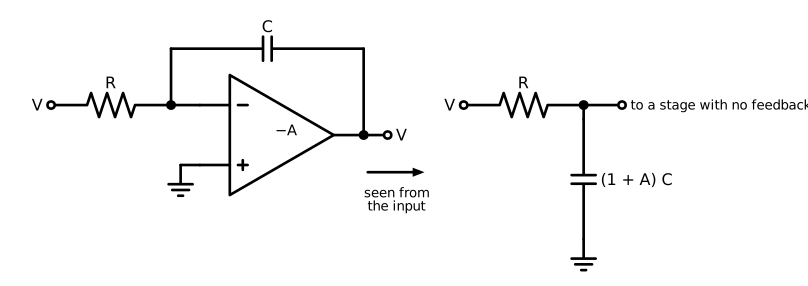 Figure 3. Miller effect. From the input side, a capacitor bridging an inverting gain of A appears multiplied by 1 + A. The source resistance and that multiplied capacitance set the corner.
Transistors by inspection
The first question about any transistor is what sets its current. The answer is nearly always a resistor at the emitter or source together with a voltage at the base or gate, or a current mirror, or a load. Find that, and the operating point follows; then the small-signal parameters follow from the current.
For a bipolar transistor:
- V, changing by about 60 mV per decade of collector current and by mV per °C.
- . Base current is and only matters where it loads a high-impedance bias network; of 100 is a safe planning number.
- The intrinsic emitter resistance is : 26 Ω at 1 mA, 2.6 Ω at 10 mA, 260 Ω at 100 µA. This is the number that turns DC into gain.
- Common emitter with an emitter resistor : gain , input impedance in parallel with the bias network, output impedance . Bypass with a capacitor and the AC gain rises to above the bypass corner.
- Emitter follower: gain slightly less than 1, input impedance , output impedance .
- Common base: gain non-inverting, input impedance ; the cascode's upper device.
For a MOSFET:
- Transconductance where is the overdrive, typically 0.1 to 0.5 V; of 1 to 10 mS per milliamp for small parts. The MOSFET analog of is .
- Common source with a source resistor: gain . Without: .
- Source follower: gain , output impedance .
- The gate draws no current, so input impedance is the bias network and the gate capacitance; the Miller-multiplied gate-drain capacitance is what limits bandwidth.
For any switch, whether transistor or MOSFET: is it fully on or fully off at every point of the cycle, what is the voltage across it in each state, and what is the current through it. The product of those in the transition is the switching loss; the product in the on state is the conduction loss.
A diode in a signal path is a resistor of at its operating current plus a fixed drop; the same rule as the transistor, because it is the same junction.
Bode sketching
The frequency map turns into a Bode plot with three rules:
- Start at the gain in the lowest band. For a low-pass that is the DC gain; for a high-pass it is zero and the first move is upward.
- At each pole (a corner where a capacitor to ground starts to short, or a series inductor starts to open, or a series capacitor is done shorting) the slope drops by 20 dB per decade and the phase moves by , spread over a decade on either side.
- At each zero the slope rises by 20 dB per decade and the phase moves by .
Adjacent corners add: two poles a decade apart give a 40 dB per decade slope after the second. A pole and a zero a decade apart give a shelf. Resonant pairs give 40 dB per decade at once, with a peak of at the corner if exceeds about 0.7.
Reading the plot backward is the same skill. A response with one corner is a single RC or L/R and the corner gives the product. A response falling at 40 dB per decade has two reactive parts in play. A phase of at a frequency where the magnitude is still flat means a pole is coming within a decade.
For stability, the loop gain of a feedback system is read the same way, and the question is the phase at the frequency where the loop gain crosses 1. Each pole inside the loop costs 90° eventually, and a loop with two poles well below the crossover is at the edge; a loop with three is an oscillator. That is the entire reason op-amps are internally compensated to a single dominant pole, and the reason a capacitive load, which adds a pole with the output impedance, causes ringing.
Time domain by inspection
A step applied to an RC or L/R circuit produces an exponential with time constant or . Three numbers cover most estimates: 63 % of the way at , 95 % at , 99 % at . The rise time from 10 % to 90 % is , and a circuit with a dB bandwidth of has a rise time of . A 1 MHz bandwidth is a 350 ns rise time.
An LC pair, or any second-order circuit, rings at with an envelope that decays in about cycles. below 0.5 gives no overshoot; of 1 gives about 16 %; of 5 gives about 70 %, and the ringing is visible for a couple of microseconds at 1 MHz.
A capacitor charged by a constant current ramps at : 1 mA into 1 nF is 1 V/µs. An inductor with a constant voltage across it ramps its current at : 12 V across 100 µH is 120 mA/µs. These two relations are the whole of switching converter analysis, and of slew rate, and of the "how long does this take" question generally.
Steady state is the question "what does this circuit do when nothing is changing", and it is the DC analysis again: capacitors open, inductors shorted, and the transient between the initial state and that one is the exponential or the ring.
Sanity checks
An estimate that fails a sanity check is wrong. An estimate that passes all of them is usually right in structure.
- Limits. Set the frequency to zero and to infinity and read the circuit each way. Set a resistor to zero and to infinity. The answer must go to the obvious value at each limit.
- Remove the part. If a part is removed and nothing changes, either it is doing nothing or the analysis missed what it does. Both are worth knowing.
- Power. Every voltage across a resistor is a current through it and a power in it, . A number that gives a resistor watts when it is an 0402 is wrong. A supply delivering less power than the load dissipates is wrong.
- Sign. Inverting stages invert. Negative feedback reduces gain. Current flows from high potential to low through a resistor. An answer with the wrong sign is a wrong answer, not a rounding error.
- Units. A time constant is ohms times farads. A gain is dimensionless. A number in the wrong unit is not a number.
- Magnitudes. Op-amp inputs sit at microvolts of difference, transistor base-emitter junctions at 0.65 V, LEDs at 2 V, supply rails where the schematic says. A node at 47 V on a 5 V board is wrong.
- Swing. The output of anything must fit between its supplies. An op-amp asked for 12 V on a 5 V supply clips; a transistor with 0 V from collector to emitter is saturated and has no gain.
- Energy in switching circuits. Input power equals output power plus losses, so ; a boost with a gain of 3 draws three times the load current from the input, and everything on the input side is sized for that.
- Symmetry. Symmetric circuits give symmetric answers. If the two halves of a differential pair come out different, a mistake was made in one.
Worked examples
Common-emitter stage with coupling and bypass capacitors
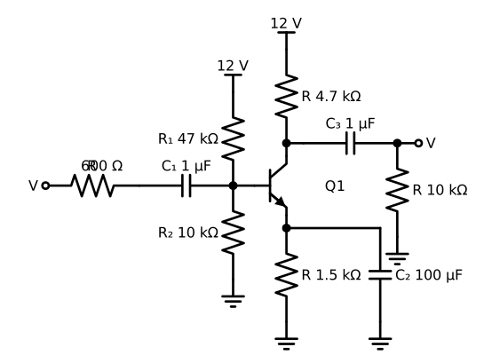 Figure 4. A common-emitter amplifier stage with input and output coupling capacitors and an emitter bypass capacitor, driven from a 600 Ω source into a 10 kΩ load on a 12 V supply.
Step 1, structure. Signal enters through to the base, leaves through from the collector; the emitter has with across it; and bias the base from the 12 V supply. A single inverting gain stage, AC coupled at both ends, with a bypassed emitter.
Step 2, DC. All three capacitors are open. The base sits at the divider: 47 kΩ over 10 kΩ from 12 V gives V, and the divider's Thevenin resistance is kΩ; base current at 1 mA and is 10 µA, dropping 80 mV across that, so call the base 2.0 V. The emitter is 0.65 V below: 1.35 V across kΩ gives mA. The collector is V. Everything is in the active region with 6.4 V of collector-emitter headroom. Ω.
Step 3, the frequency map. µF sees the source resistance plus the input impedance of the stage. Above the emitter bypass corner the input impedance is kΩ kΩ, so works against about kΩ: corner near 59 Hz. µF sees kΩ: corner near 11 Hz. µF sees the resistance looking into the emitter, Ω, in parallel with : about 100 Ω, corner near 16 Hz; below it the gain is the unbypassed , above it the bypassed . Sorted: 11 Hz, 16 Hz, 59 Hz. Below 11 Hz nothing passes. Between 60 Hz and the transistor's own limits the stage is in its midband. The three corners are within a factor of six, so the low-frequency roll-off is a rounded shoulder from about 10 to 100 Hz rather than three distinct breaks.
Step 4, midband. All three capacitors are shorts. The emitter is at AC ground. Collector load is kΩ. Gain from base to collector is . The source divider, 600 Ω into 2.1 kΩ, loses 22 %, so the overall midband gain is about , 39 dB.
Step 5, high-frequency limit. The Miller-multiplied collector-base capacitance, a few picofarads times a gain of 110, is several hundred picofarads at the base, working against Ω: a corner in the low hundreds of kilohertz. That, not the transistor's transition frequency, is the top of the band.
Step 6, checks. Gain limits: with unbypassed the gain would be ; the bypass capacitor buys a factor of 35 at the cost of the 16 Hz corner and of input impedance. Swing: 85 times a 50 mV input is 4.2 V peak, within the 6.4 V of headroom on the collector side and the 7.8 V on the other. Power: 0.9 mA at 12 V is 11 mW total. Remove the part: removing drops the gain to 3 and raises the input impedance to kΩ kΩ kΩ; both are consistent with the map.
Sensor divider into an ADC through an RC filter
A resistive sensor of 10 kΩ nominal in a divider with a 10 kΩ reference resistor from a 3.3 V supply, through a 10 kΩ series resistor and a 100 nF capacitor to ground, into an ADC input that draws 1 µA and samples in 1 µs from a 10 pF hold capacitor.
Structure: divider, RC low-pass, sampled load.
DC: the divider gives 1.65 V at 10 kΩ. Its Thevenin resistance is kΩ. In series with the 10 kΩ filter resistor, the ADC sees 15 kΩ. The ADC's 1 µA of leakage drops 15 mV across that, about 0.5 % of full scale and 4.6 LSB at 10 bits; it is the largest DC error in the chain and it must be either budgeted or removed with a buffer.
Frequency map: the 100 nF capacitor sees 15 kΩ: corner at 106 Hz. Below that the ADC sees the divider; above it the capacitor holds the node. Any interference above a few hundred hertz is attenuated by the ratio of corner to frequency: 50 kHz switching noise is down by about 470, 53 dB.
Sampling: when the ADC connects its 10 pF hold capacitor, the 100 nF supplies the charge with a 1:10000 ratio, so the node droops by 1.65 V / 10000 = 165 µV, 0.05 LSB, and recovers through 15 kΩ and 100 nF, a 1.5 ms time constant, which is far slower than the 1 µs sample but irrelevant because the droop was negligible. The 100 nF is the charge reservoir; that is its second job.
Checks: remove the capacitor and the ADC's 10 pF must charge through 15 kΩ in 1 µs, a time constant of 150 ns, 6.7 time constants, settling to 0.1 %; workable but with no interference rejection. Remove the 10 kΩ and the corner moves to 318 Hz and the leakage error halves. Every part has a stated reason.
Practice drills
Skill at inspection is built by doing the six steps on circuits whose answers are known, until the steps run without being named. A routine:
- Take any schematic and, in one minute, write the DC voltage at every named node. Then check with a simulator or a calculation. Repeat until the numbers agree within 20 % on the first pass.
- For any circuit with capacitors, write the sorted list of corner frequencies from the 159 rule without a calculator. Then check.
- Sketch the Bode magnitude plot from the corner list before simulating. Compare slopes and corner positions, not exact values.
- For any amplifier, write the gain as a ratio of two resistances, then the input and output impedance as Thevenin resistances. Check with the simulator's AC analysis.
- Pick one part and predict what changes if it is doubled, halved, or removed. Then try it.
- Explain the circuit in three sentences to someone who has not seen it. If the explanation needs a fourth sentence, a step was skipped.
The simulator is the answer key, not the method. The point of the method is to know what the simulator will say before it says it, and to notice when it says something else.
Numbers to memorize
| Quantity | Value |
|---|---|
| 0.159 | |
| Reactance of 1 µF at 1 kHz | 159 Ω |
| Reactance of 1 mH at 1 kHz | 6.28 Ω |
| RC corner of 1 kΩ and 1 µF | 159 Hz |
| LC resonance of 1 µH and 1 µF | 159 kHz, Ω |
| of a bipolar junction | 26 mV / ; 26 Ω at 1 mA |
| 0.65 V, 60 mV per decade, mV/°C | |
| MOSFET | |
| Rise time from bandwidth | |
| Exponential settling | 63 % at , 95 % at , 99 % at |
| 3 dB | factor of 1.41 in voltage, 2 in power |
| 6 dB | factor of 2 in voltage |
| 20 dB | factor of 10 in voltage |
| One pole | dB per decade, dB per octave, |
| Thermal noise of 1 kΩ at 25 °C | 4 nV/√Hz |
| Capacitor ramp | |
| Inductor ramp | |
| Trace inductance | about 1 nH/mm |
| Capacitor lead inductance | 1 to 2 nH |
| Loaded divider | , |