Introduction
As humanity continues to develop its technology, our reliance on digital information becomes more and more prominent. This digital information can manifest as a document of text, audio, images, videos, or bring life to a much more complex electro-mechanical system. It is the life blood of automation, it helps us fly our airplanes, maneuver our cars, and allows our economy and markets to function. We use this digital information for leisure and for work, and it’s hard to look around a home or work space today and not see its abundant presence.
At the heart of these different manifestations of digital information are streams of bits, zeros and ones. These bits are used to convey meaningful information. It must be this way due to the binary nature of the logic structures that allow digital computers to process information and make decisions. There are two big players in today’s methods of digital computing, general purpose processors and application specific digital circuits. The reason these two methods exist are because neither one is particularly good at doing what the other one does best.
A general purpose processor is excellent at making decisions and scheduling tasks. Its hardware is defined and so are the instructions it can interpret. It relies on a manmade program that resides in its memory, in which it is able to fetch the instructions from and perform the requested action. It is sequential in nature in that it must fetch an instruction, decode it, do the action requested (manipulate data), and proceed to the next instruction until the end of the program is reached. This method is desirable in that it makes it relatively easy to implement complex decision making trees which would otherwise require a very cumbersome finite state machine.
Application specific digital circuits are digital hardware that have been designed and optimized to perform one and only one task extremely well. It does not rely on instructions, rather, it is fed digital information at its input and a clock keeps cadence for the information as it propagates through the logic fabric towards the output. Because it does not need to fetch instructions in a sequential manner, there are many opportunities to pipeline certain processes and run multiple processes in parallel. For this reason, it is highly desirable to apply this method of computing to tasks that are computationally complex but redundant, such as encryption, image and video compression, software defined radio, wireless communication, networking, high frequency trading, and computer vision.
These circuits can be realized in a permanent optimized form, known as an ASIC (Application Specific Integrated Circuit), or as a malleable, re-configurable fabric known as an FPGA (Field Programmable Gate Array). While a general purpose processor and an ASIC/FPGA can do the same task, it is valuable to know when to employ one or the other, or both, as a solution for a project.
Xilinx ZYNQ 7000 SoC
The Xilinx ZYNQ could be considered a heterogeneous computer in that it combines both of the previously mentioned realizations of computing within a single package of silicon. This affords the designer the best of both worlds when dealing with systems that could benefit from the decision making abilities of a general purpose processor and the sheer computational power of application specific logic circuits. Within the Xilinx ZYNQ SoC is a hard processor consisting of two ARM Cortex A9 cores and a section dedicated to logic fabric much like what is found in a traditional FPGA. With this, the processing system (PS) can run bare metal or with an operating system, and is afforded the luxury of off-loading computationally intensive operations to hardware that is defined in the programmable logic (PL).
Here is a high level overview of the ZYNQ 7000’s architecture:
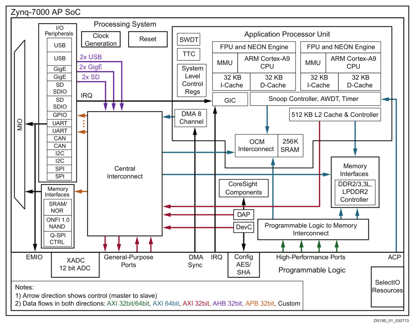
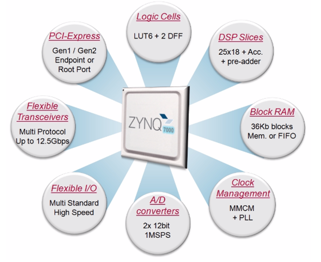
Programmable Logic
The programmable logic on the Zynq 7000 is available to extend the capabilities the processing system by hosting hardware accelerators or peripherals, which are commonly referred to as intellectual property (IP). It is connected to the PS with 9 AXI interfaces and over 3000 interconnections. The amount of programmable logic available is dependent upon the class of Zynq chip. Programmable logic, at a high level, is a matrix of resources connected to one another for a broad mesh of configurable interconnections. Within this matrix, various digital functions can be designed and implemented. The basic building block of these matrices are logic cells, each consisting of a 6 input look up table with dual flip flops. The Xilinx architecture also allows for these building blocks to also be turned into small distributed memory, shift registers, or other combinatorial functions.
Another resource within the PL are the DSP blocks. The DSP blocks are small but powerful MAC engines consisting of a 25×18 bit multiplier with a 25-bit pre-adder, followed by a 48-bit ALU and 96-bit accumulator. These blocks are intended for signal processing functions and filtering. Another important element of the PL is the block ram (BRAM). These are configurable 36 kb memory blocks can support memories from 1 bit up to 72-bits wide. They can be configured as single port or simple/true dual port memory. These blocks can be combined together to build larger memory or FIFOs. Lastly, the PL contains many clocking resources, such as mixed mode clock managers, PLLs, and regional and global clock buffers. The PL can be configured by use of an HDL (VHDL/Verilog), Vivado HLS (C/C++), Mathworks (MATLAB/Simulink), or LabVIEW.
Processing System
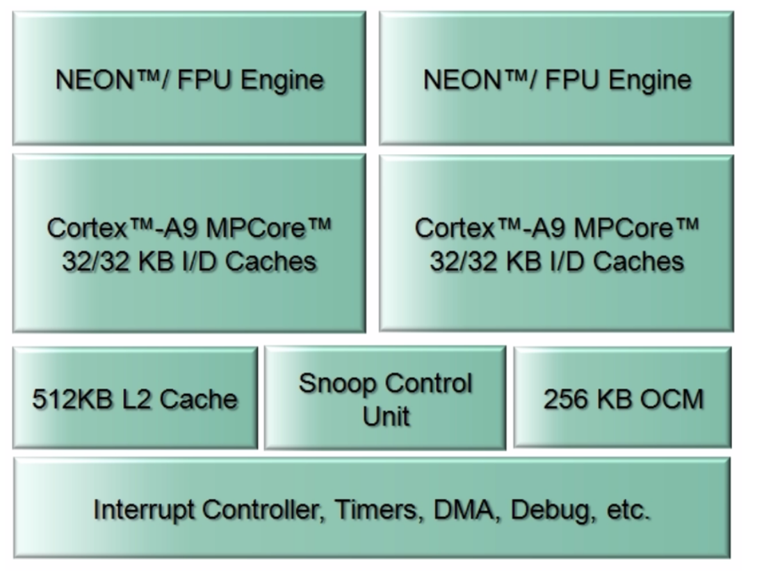
The processing system within the Zynq 7000 consists of a dual core ARM Cortex A9, each with their own L1 cache memory. On the 7020 device featured on the popular ZedBoard, the cores can be clocked up to 866 MHz and can support 128 I/Os. Additionally, it contains everything that is needed to run an operating system on a single core. Each core has its own NEON engine for multimedia applications and vector FPU engine for single and double precision. The cache currency between the two cores is controlled by the Snoop Control Unit. Both of the cores share 512KB of L2 cache and 256KB of on chip memory.
To complete the PS are standard peripherals such as interrupt controllers, timers, DMA, and debug. When the Zynq is initially powered, the processing system is the first to boot and will decide what will happen. The bit streams for the programmable logic can be stored on an SD card or within flash memory, and the PL fabric can be configured by the PS upon booting. Other key peripherals that are supported are USB 2.0, Gb Ethernet, SD/SDIO, CAN, I2C, I2S, SPI, UART, and XADC. The Zynq processing system can be implemented as bare metal (no OS), with an operating system, or both.
AXI Interface
In order for the PS to communicate with hardware peripherals that are instantiated within the PL, a communication protocol that allows for both the PS and PL to access the share information within DDR3 memory in a managed and timely manner must be implemented. This communication protocol is an industry standard known as AXI4 (Advanced eXtensible Interface 4). All of the IP blocks that are designed for a Zynq 7000 chip are created as AXI masters or slaves.
Three types of AXI can be implemented, namely, high performance memory mapped interface, lite memory-mapped interface, and stream interface. The stream interface is a reduced version of the memory mapped interface. The AXI master has the ability to initiates read and write commands, while the slave can only respond to these commands. The Xilinx AXI Interconnect IP contains a configurable number of AXI-compliant master and slave interfaces, and can be used to route transactions between one or more AXI masters and slaves.
In memory-mapped protocols, all transactions involve the concept of transferring a target address within a system memory space, where the IP operates in a defined memory map. For this reason, when implementing a hardware peripheral or accelerator, it must include the necessary I/O to allow it to join the AXI bus.
Software Design Tools
Xilinx provides a software package capable of managing every stage of design for the Zynq SoC. The Vivado Design Suite consists of three major components, namely Vivado, HLS (High-Level Synthesis), and SDK (Software Development Kit).
Vivado HLS
Vivado HLS is a software package that allows for IP to be implemented in C or C++. Traditionally, hardware is created using a hardware description language such as VHDL or Verilog. The advantage that HLS provides is that it allows the designer to describe the algorithm in a familiar manner using C/C++ which will then be automatically translated to VHDL or Verilog. There are further features within HLS that allows for loop and function optimization. A test bench for proving out the functionality of the hardware can also be developed in C or C++. With that being said, HLS’s easing of the development process comes at the expense of control.
There are applications where the designer cannot afford to have HLS do its work behind the curtains and must manually write the HDL. It should be noted that Vivado HLS will not accept just any C code. C code that attempts to allocate dynamic memory cannot be used in HLS, all memory instances must be static. Additionally, no system calls such as std or file I/O can be used, and recursive functions should be avoided. Additionally, the HDL that is generated by HLS will not as “readable” as if it were written by a human.
Vivado IP Integrator
Vivado IP integrator is used to define the PL and PS connections and interfaces in a way similar to what is found in Mathworks Simulink. A block diagram is created where all of the IP can be dropped into and connected with other IP cores or processing systems. Once the connections have been finalized, a high level HDL wrapper is created and used to generate a bit stream. Once the bit stream has been generated, the design moves over to Xilinx’s SDK.
Xilinx SDK
Xilinx SDK is used to program the ARM cores. As mentioned before, the ARM cores can run a bare metal application, an operating system, or both. Because the Zynq is a processing centric system, this is an absolutely crucial piece of the design process. The ARM cores can be programmed in C and have access to user customizable libraries and hardware drivers. The SDK IDE provides true homogenous and heterogeneous multi-processor design and debug capabilities.