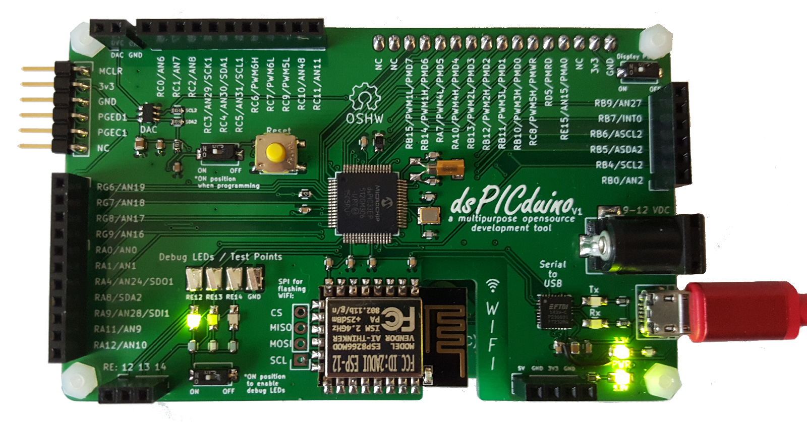
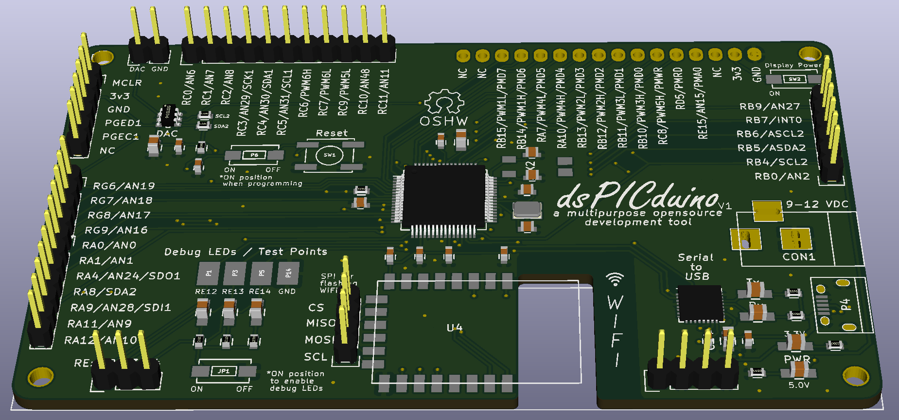
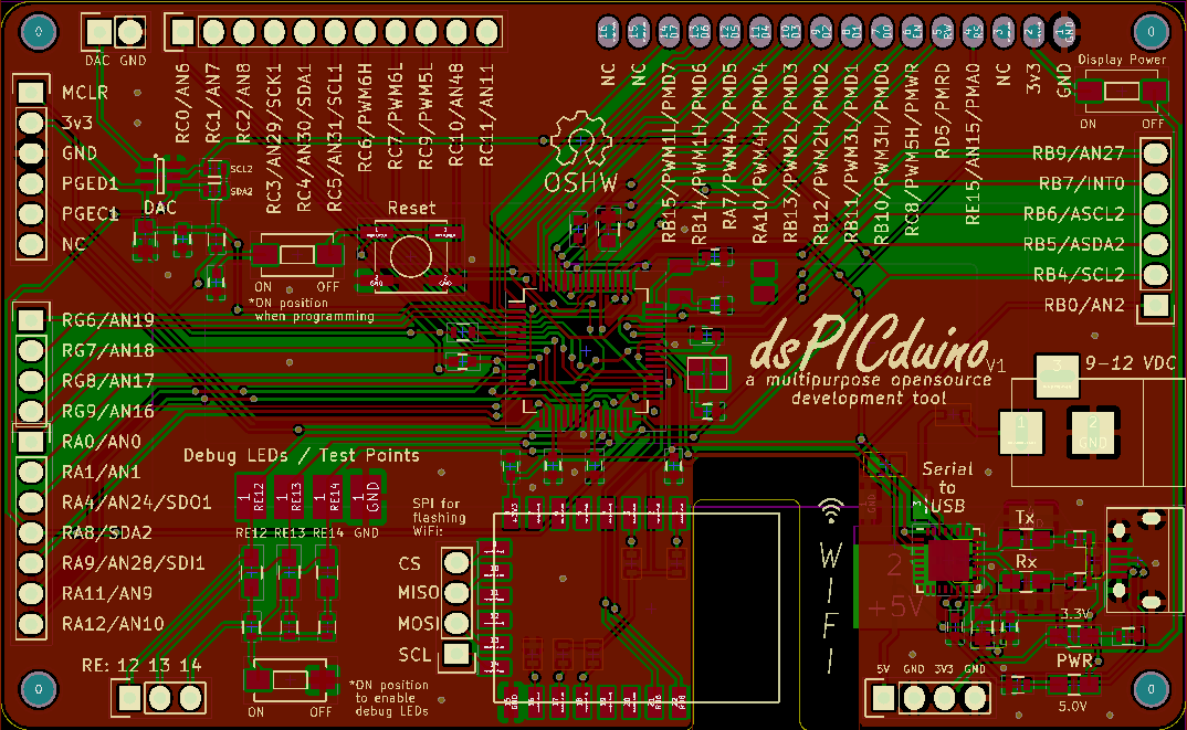
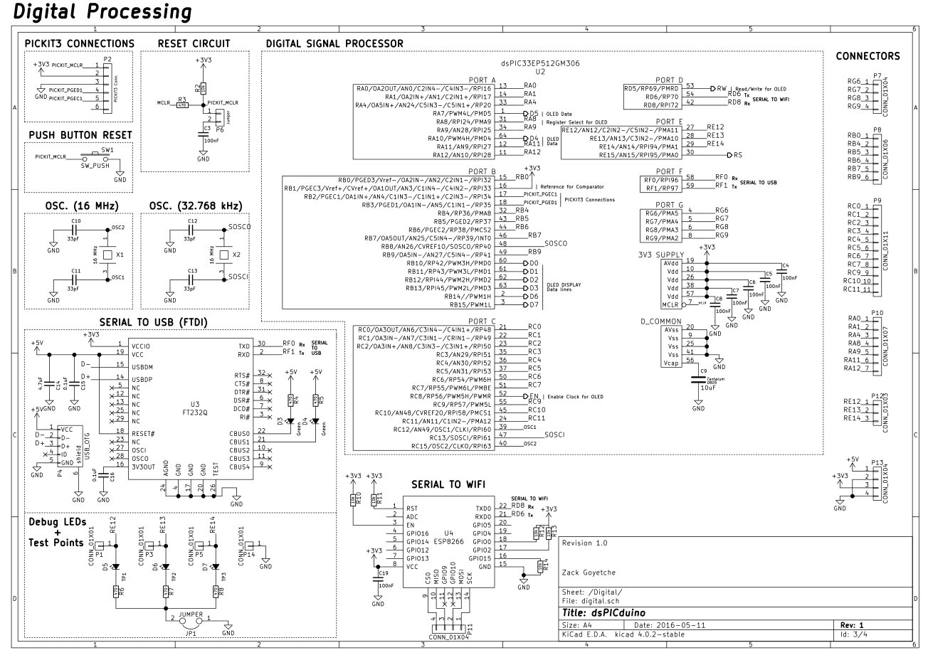
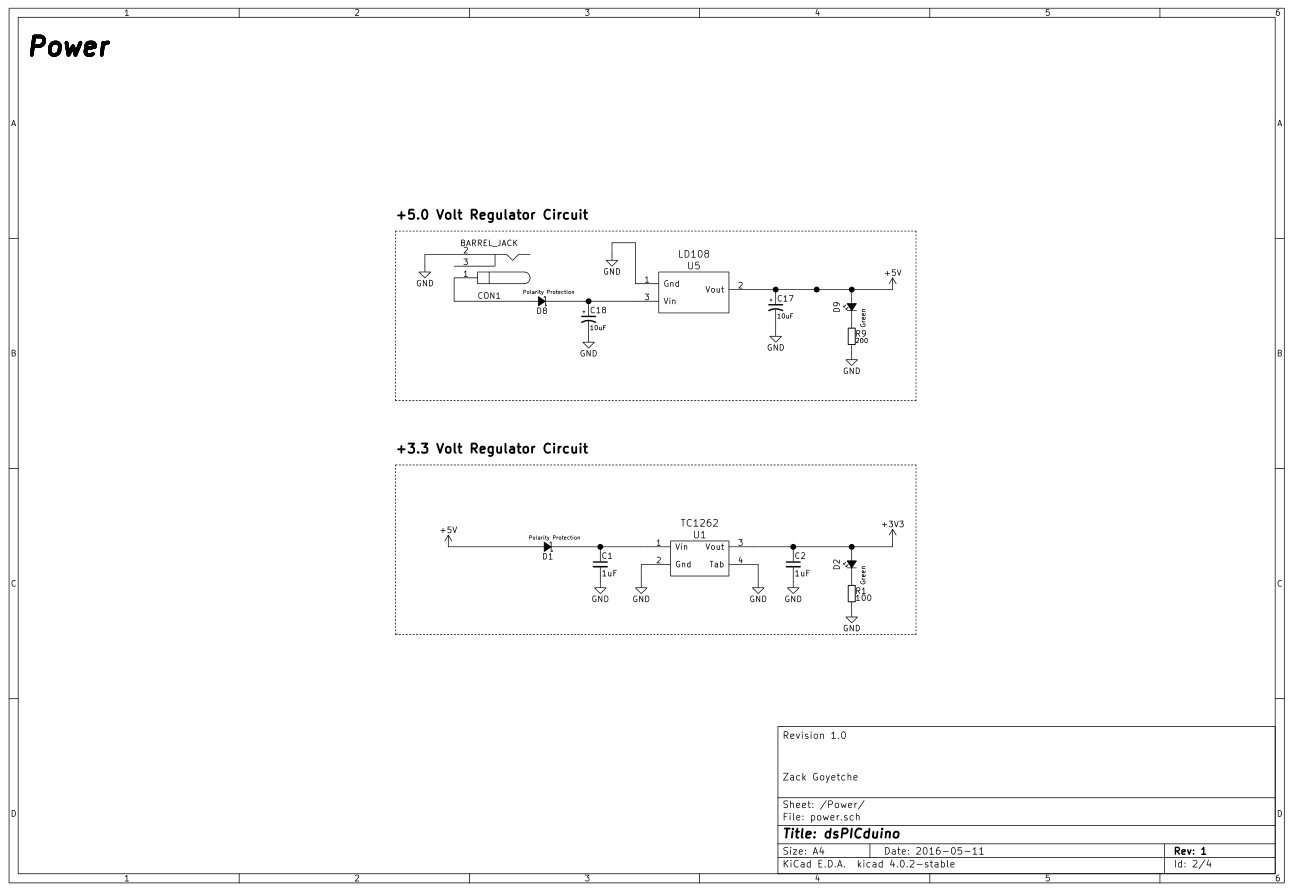
As an attempt to start an open source project, I’ve designed a general purpose development board featuring Microchip’s dsPIC along side the ESP8266.
The Arduino has gained immense popularity due to its ability to allow hobbyists to incorporate embedded control/processing into their projects. I am grateful for the Arduino, as it inspired me to explore the field of embedded hardware and software design.
The purpose of the dsPICduino is similar to the purpose of the Arduino — that is, it serves as both a learning and development platform for the aspiring embedded developer. The dsPICduino offers a more immersive embedded experience by stepping away from the layers of abstraction provided by the Arduino ecosystem.
Features of the dsPICduino
WiFi station capability (ESP8266 running NodeMCU)
Break out of 42 general purpose digital I/O pins
Break out 15 analog channels
Break out of 12 high speed PWM channels
12 bit DAC (accessable via I2C)
Break out of hardware SPI and I2C busses
USB to serial converter (FTDI)
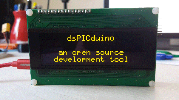
Easily integrated to character/matrix displays via Parallel Master Port
Debugging LEDs and test points
Secondary tuning fork oscillator (32.768 kHz) for real time clock/calendar
(9) 16-bit timers, or (1) 16-bit and (4) 32-bit timers
Hardware Output Compare and Input Capture
Motor Control Peripherals with fast and flexible PWMs
1MSPS 12bit ADC or (32) multiplexed analog inputs @ 10-bit
SPI, I2C, CAN, UART
Demonstrations
With WiFi and USB incorporated into the dsPICduino, projects can be easily integrated into IoT applications. The following GIFs demonstrate utilization of the USB to serial converter allowing a user to configure the WiFi module to connect to their local network.
Once connected, the WiFi module acts as a station on the network with internet access. From here, HTTP GET requests can be made to then scrape and parse HTML for weather and UNIX time data.
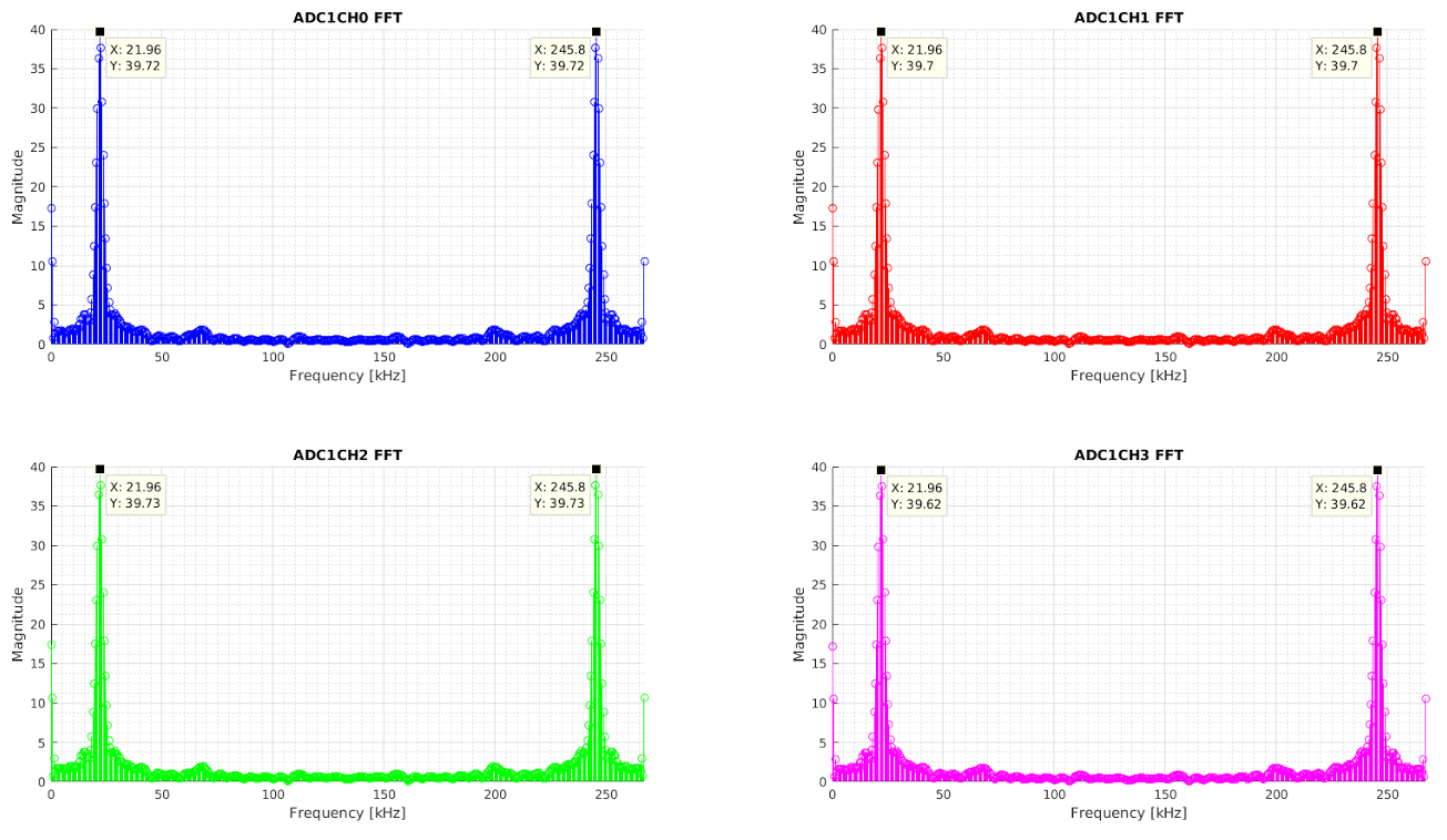
All of this functionality is complemented by the dsPIC’s ability to perform DSP functions that are useful in signal processing applications such as audio, motor control, and RF.
The following image is a plot of the magnitude of the complex array returned by the dsPIC (off loaded through the debugger) when using it to compute the FFT of a sampled 22 kHz sinusoidal signal on 4 analog channels.
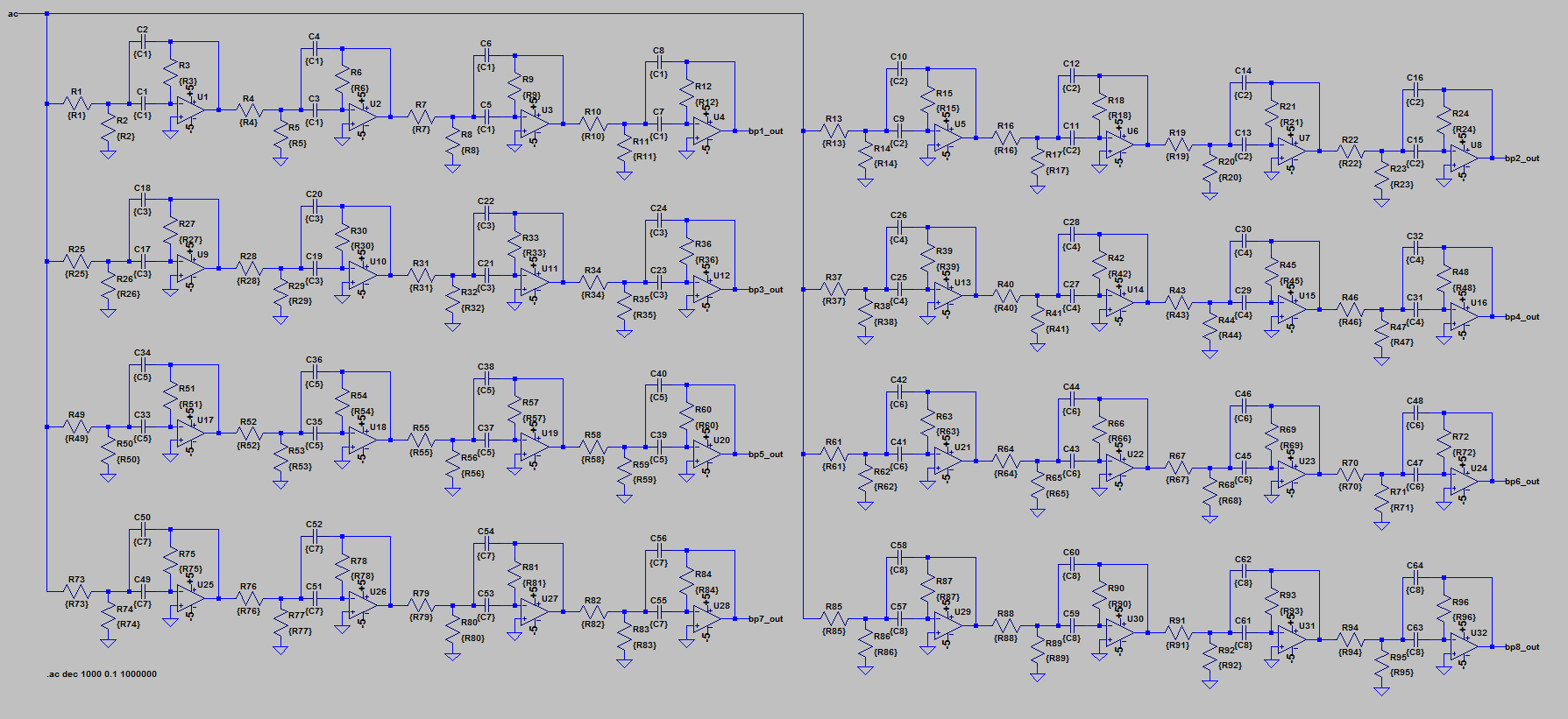
Analog filter design can be a tedious task, requiring frequency transformations, pages and pages of algebra, and many simulations to check that you are getting the response you designed for. Through the use of Geffe’s algorithm and Delyiannis-Friend circuits, bandpass filter design can be partially automated.
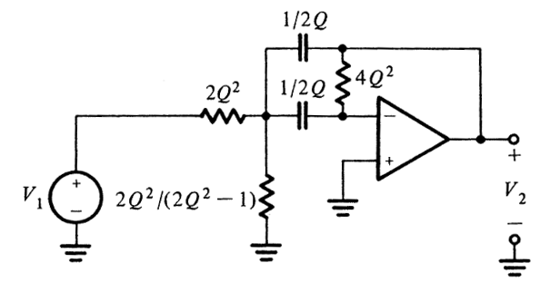
Delyiannis-Friend circuit with unity gain [1]:
The purpose of this post isn’t to detail the specifics behind Geffe’s algorithm, but rather to share with you a python script I wrote that will apply Geffe’s algorithm to a given set of input parameters, and output the required component values for each Friend circuit.
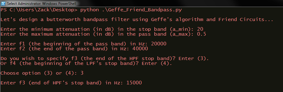
It is required that you have Python3 along with numpy, matplotlib, and scipy installed on your machine. The script can be executed through the Powershell if you are a Windows user by navigating to the directory where the Geffe_Friend_Bandpass.py file is located and then typing: python .\Geffe_Friend_Bandpass.py
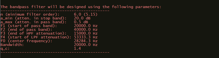
Upon execution, the python script will prompt you for some input parameters.
You are first asked for the maximum attenuation in the stop bands and the minimum attenuation in the pass band.
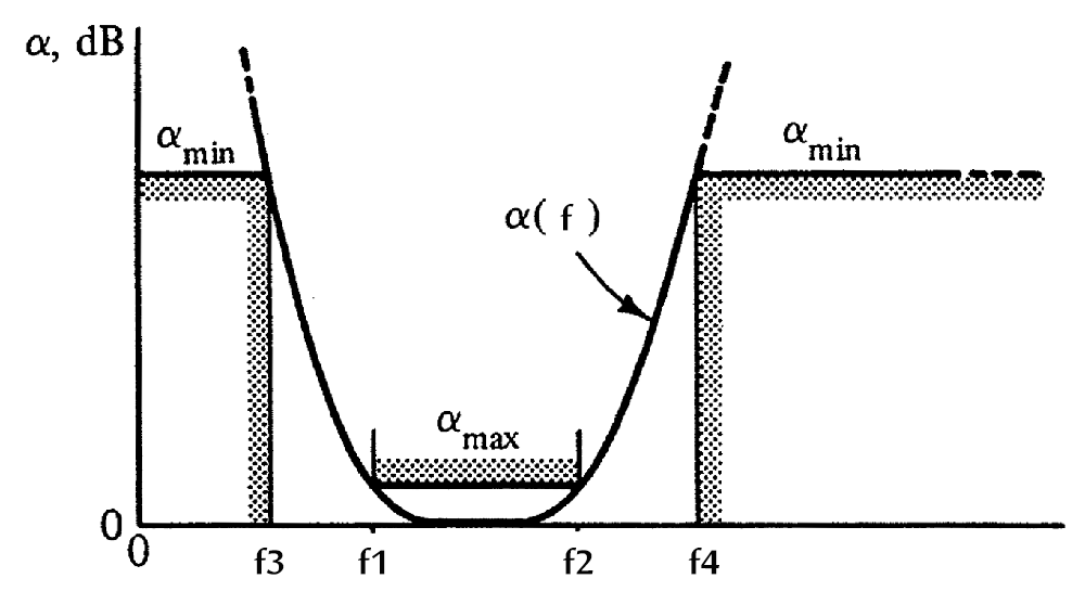
Then, you are asked to specify the pass band frequencies (f1 and f2) and one of the stop band frequencies (f3 or f4). The other stop band frequency is solved for automatically. See the following image [1]:
Parameter Details
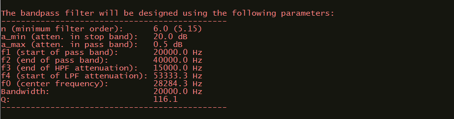
The script will then return to you the information you had just entered, along with the minimum order filter required to meet your specifications.
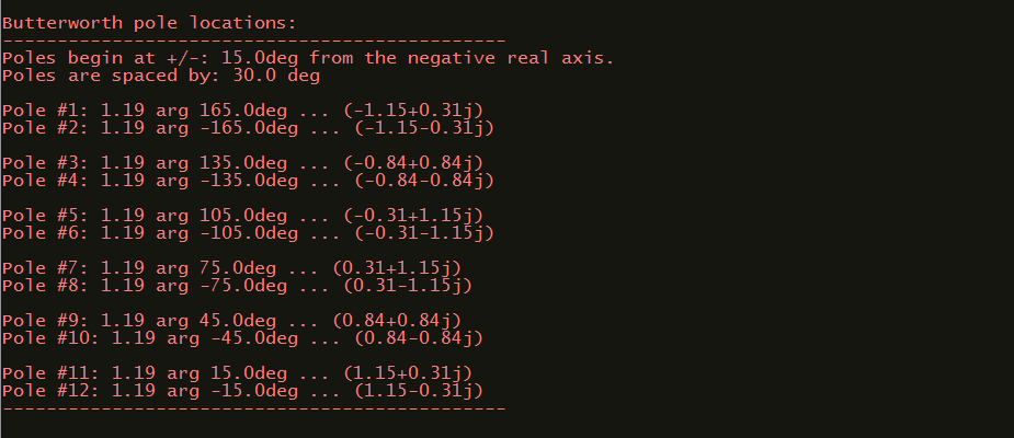
Butterworth Pole Locations
The locations of the poles are returned in both polar and rectangular format.
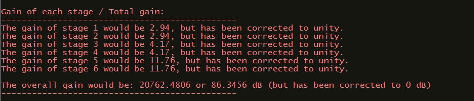
Gain Information
The gain of each stage is normalized to unity, resulting in unity gain at the center frequency.
The script can be tweaked to create a filter/amplifier, or an additional amplifier can be added after the filter.
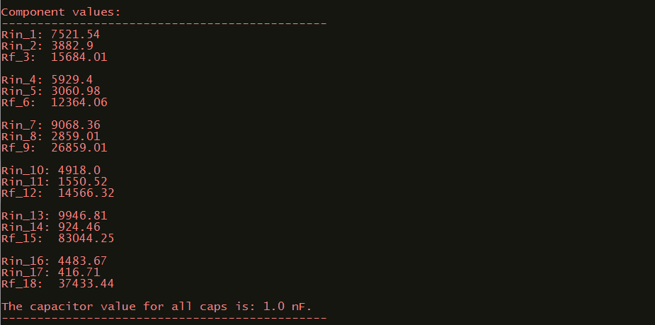
Required Resistor and Capacitor Values
The script will automatically calculate reasonable component values for each Friend circuit.
Note that n operational amplifiers (Friend circuits) are required for an nth order filter.
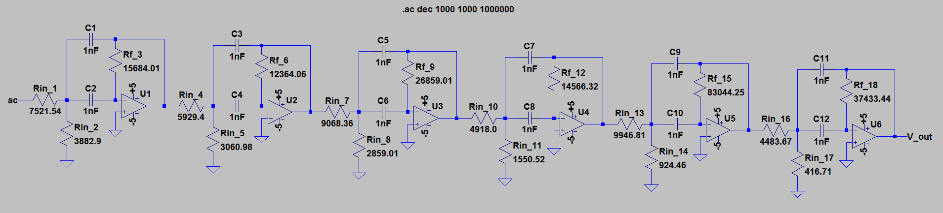
Click on the image to enlarge it, notice how the resistors and capacitors correspond to the output generated by the python script.
This example can be used as a general case, and the same arrangement will arise for any nth order output.
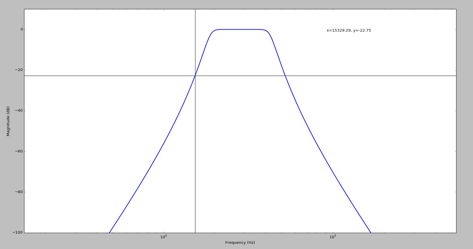
Auto Generated Bode Magnitude Plot
The script will then call on matplotlib to generate the bode magnitude plot of the filter. Interactive cursors have been added to allow for inspection of the pass and stop band frequencies.
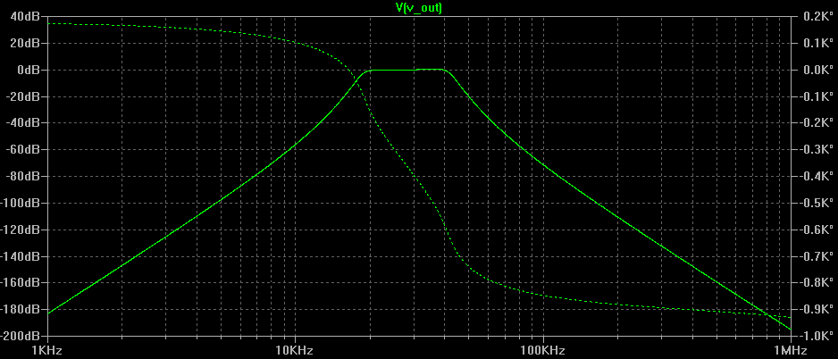
Plotting in LT Spice (AC Sweep)
Here is the frequency response of the circuit once it had been built in LTSpice:
Conclusion
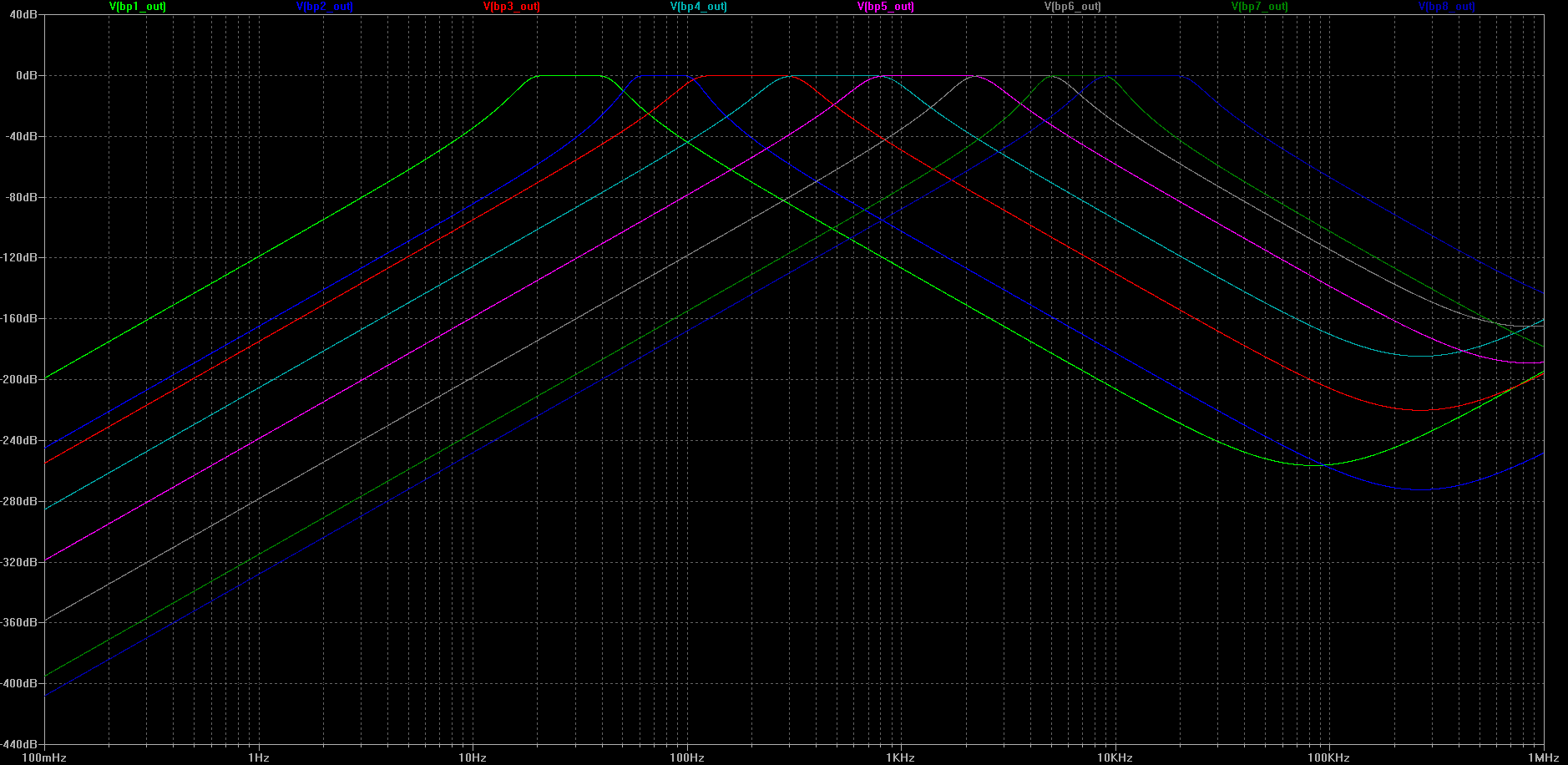
So what is this script good for? Let’s say you wanted to build a circuit that required multiple analog bandpass filters, but don’t want to crank out all the math to calculate the component values.
you would need 8-10 bandpass filters to select for various bands of the audio spectrum. You could use this script to design 8 bandpass filters very quickly!
As humanity continues to develop its technology, our reliance on digital information becomes more and more prominent. This digital information can manifest as a document of text, audio, images, videos, or bring life to a much more complex electro-mechanical system. It is the life blood of automation, it helps us fly our airplanes, maneuver our cars, and allows our economy and markets to function. We use this digital information for leisure and for work, and it’s hard to look around a home or work space today and not see its abundant presence.
At the heart of these different manifestations of digital information are streams of bits, zeros and ones. These bits are used to convey meaningful information. It must be this way due to the binary nature of the logic structures that allow digital computers to process information and make decisions. There are two big players in today’s methods of digital computing, general purpose processors and application specific digital circuits. The reason these two methods exist are because neither one is particularly good at doing what the other one does best.
A general purpose processor is excellent at making decisions and scheduling tasks. Its hardware is defined and so are the instructions it can interpret. It relies on a manmade program that resides in its memory, in which it is able to fetch the instructions from and perform the requested action. It is sequential in nature in that it must fetch an instruction, decode it, do the action requested (manipulate data), and proceed to the next instruction until the end of the program is reached. This method is desirable in that it makes it relatively easy to implement complex decision making trees which would otherwise require a very cumbersome finite state machine.
Application specific digital circuits are digital hardware that have been designed and optimized to perform one and only one task extremely well. It does not rely on instructions, rather, it is fed digital information at its input and a clock keeps cadence for the information as it propagates through the logic fabric towards the output. Because it does not need to fetch instructions in a sequential manner, there are many opportunities to pipeline certain processes and run multiple processes in parallel. For this reason, it is highly desirable to apply this method of computing to tasks that are computationally complex but redundant, such as encryption, image and video compression, software defined radio, wireless communication, networking, high frequency trading, and computer vision.
These circuits can be realized in a permanent optimized form, known as an ASIC (Application Specific Integrated Circuit), or as a malleable, re-configurable fabric known as an FPGA (Field Programmable Gate Array). While a general purpose processor and an ASIC/FPGA can do the same task, it is valuable to know when to employ one or the other, or both, as a solution for a project.
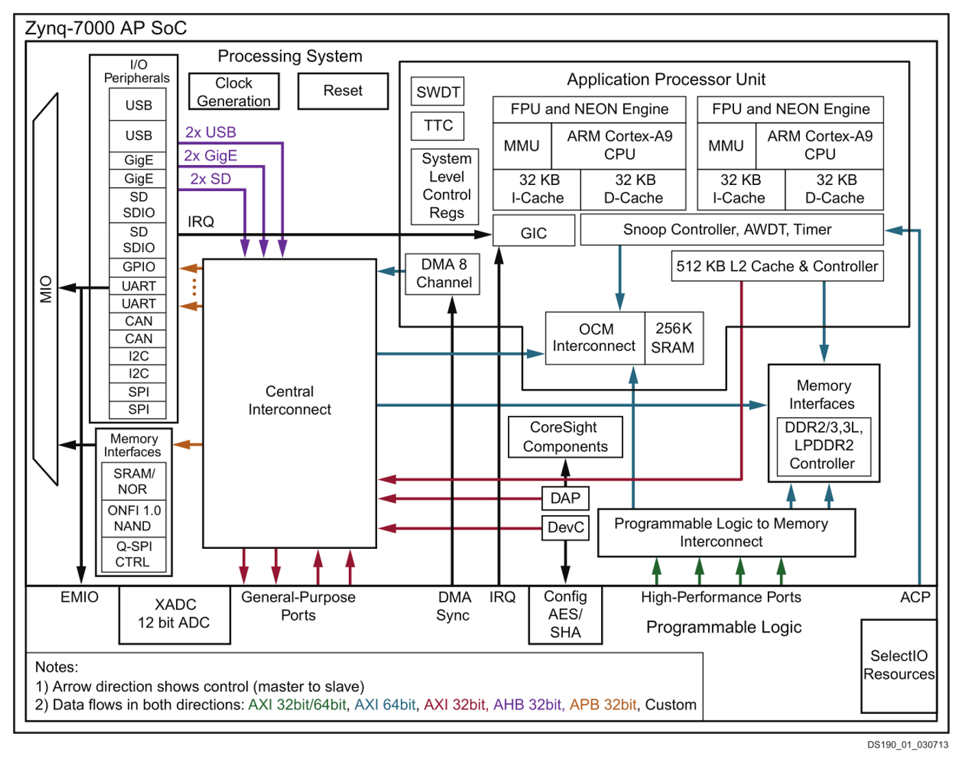
Xilinx ZYNQ 7000 SoC
The Xilinx ZYNQ could be considered a heterogeneous computer in that it combines both of the previously mentioned realizations of computing within a single package of silicon. This affords the designer the best of both worlds when dealing with systems that could benefit from the decision making abilities of a general purpose processor and the sheer computational power of application specific logic circuits. Within the Xilinx ZYNQ SoC is a hard processor consisting of two ARM Cortex A9 cores and a section dedicated to logic fabric much like what is found in a traditional FPGA. With this, the processing system (PS) can run bare metal or with an operating system, and is afforded the luxury of off-loading computationally intensive operations to hardware that is defined in the programmable logic (PL).
Here is a high level overview of the ZYNQ 7000’s architecture:
Programmable Logic
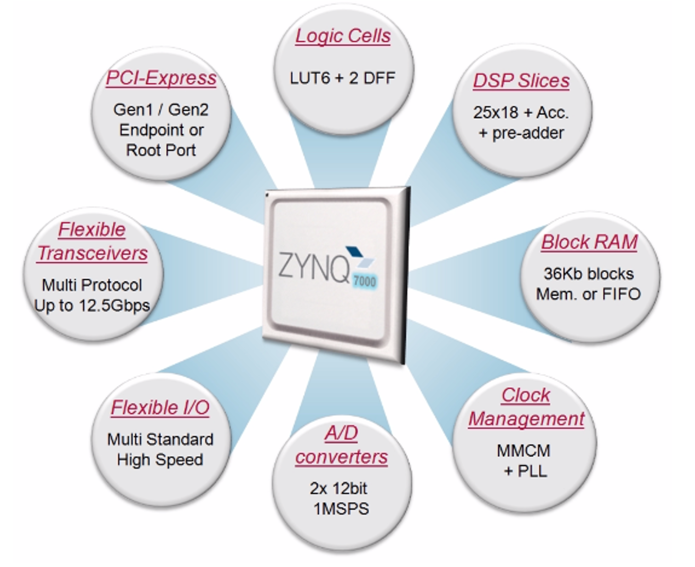
The programmable logic on the Zynq 7000 is available to extend the capabilities the processing system by hosting hardware accelerators or peripherals, which are commonly referred to as intellectual property (IP). It is connected to the PS with 9 AXI interfaces and over 3000 interconnections. The amount of programmable logic available is dependent upon the class of Zynq chip. Programmable logic, at a high level, is a matrix of resources connected to one another for a broad mesh of configurable interconnections. Within this matrix, various digital functions can be designed and implemented. The basic building block of these matrices are logic cells, each consisting of a 6 input look up table with dual flip flops. The Xilinx architecture also allows for these building blocks to also be turned into small distributed memory, shift registers, or other combinatorial functions.
Another resource within the PL are the DSP blocks. The DSP blocks are small but powerful MAC engines consisting of a 25×18 bit multiplier with a 25-bit pre-adder, followed by a 48-bit ALU and 96-bit accumulator. These blocks are intended for signal processing functions and filtering. Another important element of the PL is the block ram (BRAM). These are configurable 36 kb memory blocks can support memories from 1 bit up to 72-bits wide. They can be configured as single port or simple/true dual port memory. These blocks can be combined together to build larger memory or FIFOs. Lastly, the PL contains many clocking resources, such as mixed mode clock managers, PLLs, and regional and global clock buffers. The PL can be configured by use of an HDL (VHDL/Verilog), Vivado HLS (C/C++), Mathworks (MATLAB/Simulink), or LabVIEW.
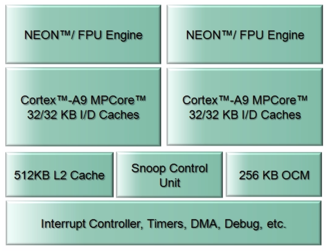
Processing System
The processing system within the Zynq 7000 consists of a dual core ARM Cortex A9, each with their own L1 cache memory. On the 7020 device featured on the popular ZedBoard, the cores can be clocked up to 866 MHz and can support 128 I/Os. Additionally, it contains everything that is needed to run an operating system on a single core. Each core has its own NEON engine for multimedia applications and vector FPU engine for single and double precision. The cache currency between the two cores is controlled by the Snoop Control Unit. Both of the cores share 512KB of L2 cache and 256KB of on chip memory.
To complete the PS are standard peripherals such as interrupt controllers, timers, DMA, and debug. When the Zynq is initially powered, the processing system is the first to boot and will decide what will happen. The bit streams for the programmable logic can be stored on an SD card or within flash memory, and the PL fabric can be configured by the PS upon booting. Other key peripherals that are supported are USB 2.0, Gb Ethernet, SD/SDIO, CAN, I2C, I2S, SPI, UART, and XADC. The Zynq processing system can be implemented as bare metal (no OS), with an operating system, or both.
AXI Interface
In order for the PS to communicate with hardware peripherals that are instantiated within the PL, a communication protocol that allows for both the PS and PL to access the share information within DDR3 memory in a managed and timely manner must be implemented. This communication protocol is an industry standard known as AXI4 (Advanced eXtensible Interface 4). All of the IP blocks that are designed for a Zynq 7000 chip are created as AXI masters or slaves.
Three types of AXI can be implemented, namely, high performance memory mapped interface, lite memory-mapped interface, and stream interface. The stream interface is a reduced version of the memory mapped interface. The AXI master has the ability to initiates read and write commands, while the slave can only respond to these commands. The Xilinx AXI Interconnect IP contains a configurable number of AXI-compliant master and slave interfaces, and can be used to route transactions between one or more AXI masters and slaves.
In memory-mapped protocols, all transactions involve the concept of transferring a target address within a system memory space, where the IP operates in a defined memory map. For this reason, when implementing a hardware peripheral or accelerator, it must include the necessary I/O to allow it to join the AXI bus.
Software Design Tools
Xilinx provides a software package capable of managing every stage of design for the Zynq SoC. The Vivado Design Suite consists of three major components, namely Vivado, HLS (High-Level Synthesis), and SDK (Software Development Kit).
Vivado HLS
Vivado HLS is a software package that allows for IP to be implemented in C or C++. Traditionally, hardware is created using a hardware description language such as VHDL or Verilog. The advantage that HLS provides is that it allows the designer to describe the algorithm in a familiar manner using C/C++ which will then be automatically translated to VHDL or Verilog. There are further features within HLS that allows for loop and function optimization. A test bench for proving out the functionality of the hardware can also be developed in C or C++. With that being said, HLS’s easing of the development process comes at the expense of control.
There are applications where the designer cannot afford to have HLS do its work behind the curtains and must manually write the HDL. It should be noted that Vivado HLS will not accept just any C code. C code that attempts to allocate dynamic memory cannot be used in HLS, all memory instances must be static. Additionally, no system calls such as std or file I/O can be used, and recursive functions should be avoided. Additionally, the HDL that is generated by HLS will not as “readable” as if it were written by a human.
Vivado IP Integrator
Vivado IP integrator is used to define the PL and PS connections and interfaces in a way similar to what is found in Mathworks Simulink. A block diagram is created where all of the IP can be dropped into and connected with other IP cores or processing systems. Once the connections have been finalized, a high level HDL wrapper is created and used to generate a bit stream. Once the bit stream has been generated, the design moves over to Xilinx’s SDK.
Xilinx SDK
Xilinx SDK is used to program the ARM cores. As mentioned before, the ARM cores can run a bare metal application, an operating system, or both. Because the Zynq is a processing centric system, this is an absolutely crucial piece of the design process. The ARM cores can be programmed in C and have access to user customizable libraries and hardware drivers. The SDK IDE provides true homogenous and heterogeneous multi-processor design and debug capabilities.
Analyzing continuous signals by means of discrete methods requires special considerations in order for the results to be meaningful and accurate. Underlying this task is an exercise of optimization, where the capturing of continuous information must be in harmony with the constraints of the digital system. The goal is to spend the least amount of computational resources required to digitally represent a continuous signal.
Throughout this exercise, theory and principles that have arisen out of a half of a century of communication systems and signal processing study will be defined, applied, and demonstrated by example through computational software.
These principles include:
Bridging the analog and digital domain using the Nyquist-Shannon sampling theorem.
Representation of discrete signals in time and frequency domain using the Fast Fourier Transform algorithm.
Defining essential bandwidth using Parseval’s theorem.
Detecting energy signals by means of autocorrelation and ESD comparison (Fourier pairs).
It will be necessary to examine signals with domains in both time and frequency, as each domain gives access to different information contained within the signal.
The Fourier Transform is a technique for mapping a function between its time/frequency or space/wavenumber domains.
The Fourier Transform is defined as follows
In everyday human experience, the signals we perceive are essentially continuous. For example, the sound waves produced by an Opera singer or heat transfer between two objects are processes which can take on an infinite number of values and exist continuously in time. This is in opposition to discrete signals which exist as packets that can take on a finite number of values and are discontinuous.
With the advent of digital computation, scientists and engineers now have the ability to solve complex problems where closed form solutions do not exist or are too difficult to obtain. In order for a digital computer to perform computations on such problems, they must be done numerically rather than analytically. For this reason, a signal that is continuous must be broken down into discrete components in such a way that its essence is captured.
Sampling, as stated previously, is the process of breaking down a continuous signal into a numeric sequence. The Nyquist-Shannon sampling theorem states that [1]:
If a function x(t) contains no frequencies higher than cps (counts per second), it is completely determined by giving its ordinates at a series of points spaced 1/2B seconds apart.
A sufficient sample-rate is therefore 2B samples/second, or anything larger. Conversely, for a given sample rate (fs) the band limit for perfect reconstruction is B ≤ fs/2.
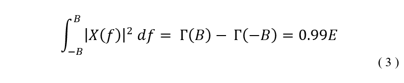
Oftentimes, it is only necessary to consider a certain range of frequencies within a signal. While a signal may theoretically have infinite bandwidth, nearly all of its energy is likely be contained within a finite bandwidth of frequencies – this frequency range is known as the essential bandwidth of a signal. To define the essential bandwidth of a signal, Parsevel’s theorem can be used to evaluate the amount of energy contained within a bound of frequencies [2].
Parseval’s theorem can be expressed as follows
What this implies is that the total energy contained within a time domain waveform summed across all time is equal to the total energy contained within that same signal’s frequency domain waveform summed across all frequencies. From this, an arbitrary variable B can be assigned to the bounds of the infinite sum and set equal to a percentage of the total energy of the signal. Using the fundamental theorem of calculus, a closed form solution can be found. Consider the following example where
The variable B can be solved for provided that the total energy E is known and |X(f)|2 is integrable. Solving for B in the example above would provide the bandwidth necessary to capture 99% of the signal’s total energy. Alternatively, the essential bandwidth can also be solved for numerically by an iterative process.
Because signals can exist in one of two forms, power or energy, it may be of interest to establish the form of a given signal. It is known that for an energy signal, its energy spectral density (ESD) and autocorrelation functions form a Fourier pair. The ESD of a signal is defined as follows
And the autocorrelation of a signal is defined as follows
If the signal x(t) is an energy signal, the resulting Fourier pair exists such that
And vice-versa
Discretization of Continuous Signals
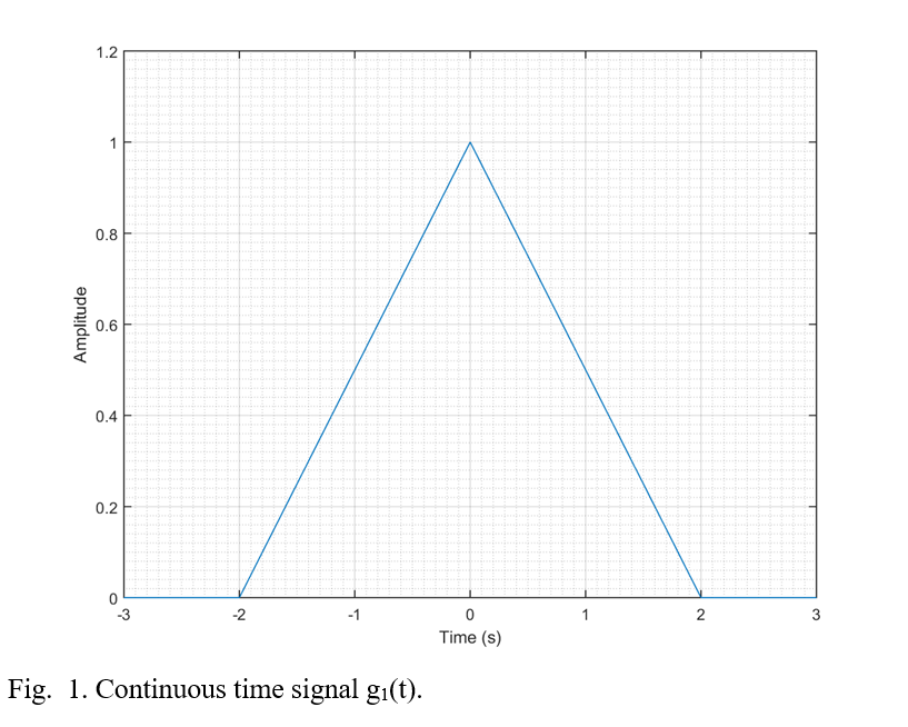
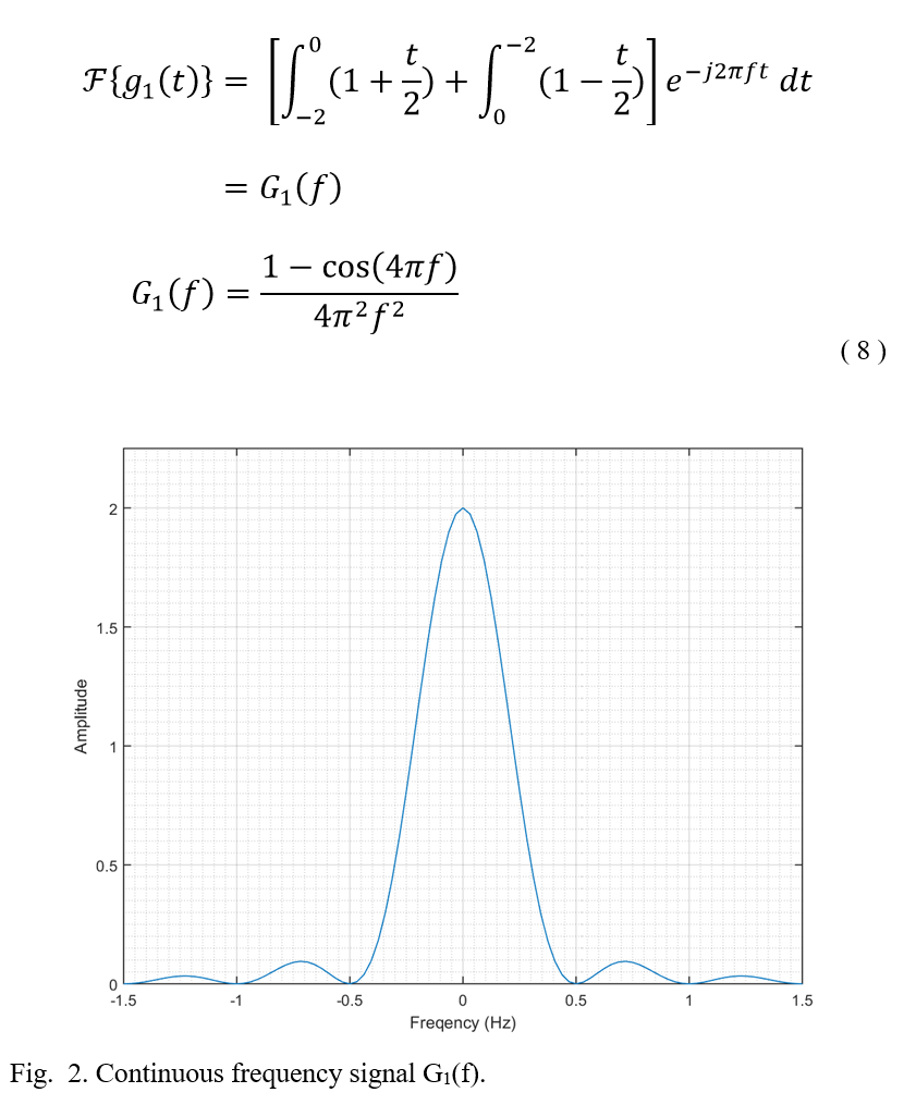
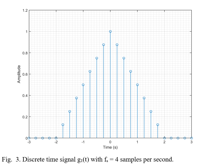
Consider the signal g1(t) = Δ(t/2) . This signal is defined for all values of time.
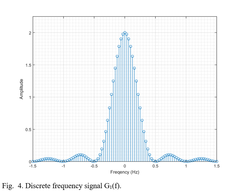
To determine the necessary sampling rate for this signal, its essential bandwidth must be established. By taking the Fourier transform of this signal, the magnitude of its frequency components will become apparent.
It can be seen in Fig. 2 that the signal’s magnitude is significantly reduced at frequencies greater than 0.5 hertz and less than -0.5 hertz.
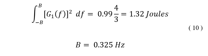
To determine this signal’s essential bandwidth, the signal’s total energy must be must be found for all frequencies.
The total energy of this signal can be found by integrating the square of the frequency components over all frequencies. From Equations (3) and (8)
It is desired to capture 99% of this signal’s energy, so by assigning a variable to the limits of integration and setting the integral equal to 0.99 times the total energy, the essential bandwidth can be found.
From this result, the Nyquist-Shannon sampling theorem suggests that a sampling frequency as low as 0.65 samples per second can be used. Because this frequency is extremely low relative to the number of instructions a modern processor can handle per second, a modest sampling frequency of 4 samples per second will be used for the following simulations.
The discrete versions of this signal at a sample rate of four samples per second can be seen in Fig. 3 and Fig. 4.
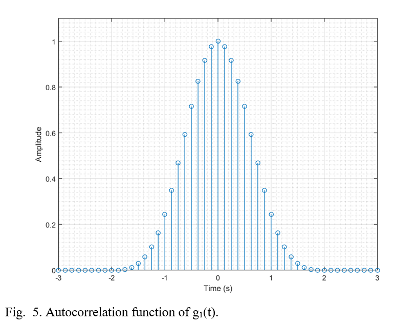
The autocorrelation function compares a time domain signal with a shifted version of itself. The resulting function is defined in Equation (5).
Performing autocorrelation on the discrete signal g1(t) results in the following time domain waveform
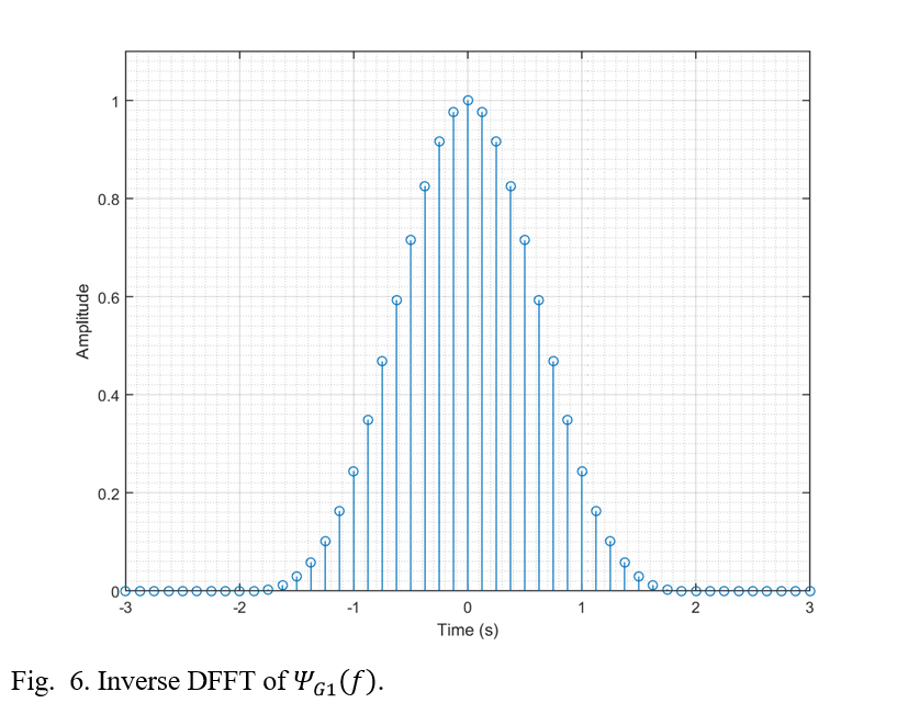
Given that g1(t) is an energy signal, the same discrete waveform should result from taking the inverse FFT of its ESD function. The ESD function is defined in Equation (4).
Performing the inverse FFT on ψg1(f) results in the following time domain waveform
It can be seen in Fig. 5 and Fig. 6 that g1’s autocorrelation function Rg1(τ) and ESD function ψg1(f) are indeed Fourier pairs.
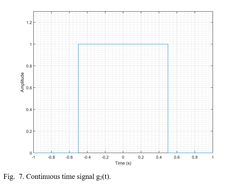
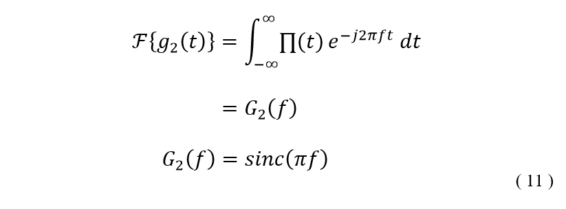
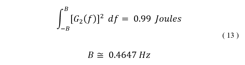
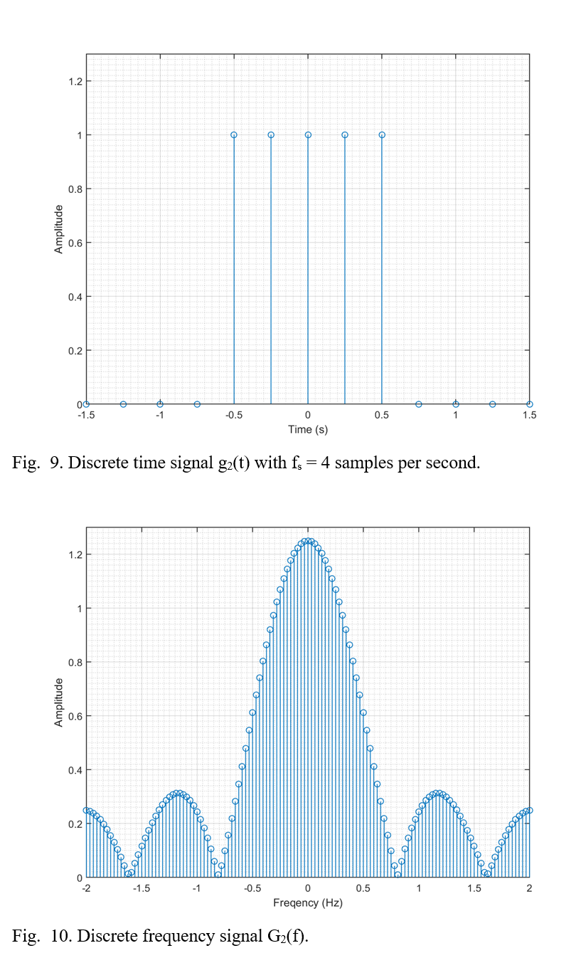
Next, consider the signal g2(t) = ∏(t) . This signal is defined for all values of time.
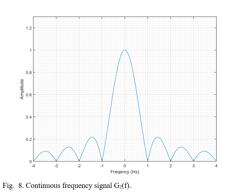
Like in the previous example, performing a Fourier transform on this signal will reveal the magnitudes of the frequency components across all frequencies.
It can be seen in Fig. 8 that the magnitude of G2(f)’s frequency components do not diminish as quickly as G1(f) did.
To find the total energy of this signal, the square of the frequency components are integrated over all frequencies. From Equations (3) and (11)
It is desired to capture 99% of this signal’s energy, so by assigning a variable to the limits of integration and setting the integral equal to 0.99 times the total energy, the essential bandwidth can be found.
To stay consistent with the previous signal g1(t), a sampling frequency of 4 samples per second will also be used for g2(t), as it exceeds the fs ≥ 2B rule established by the Nyquist-Shannon sampling theorem. The discrete versions of this signal can be seen in Fig. 9 and Fig. 10.
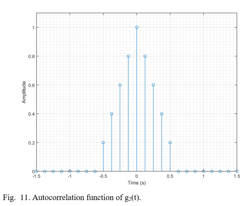
Performing autocorrelation on the discrete signal g2(t) results in the following time domain waveform
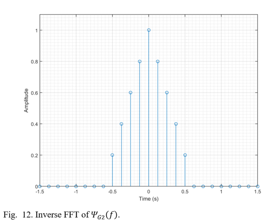
Performing the inverse FFT on ψG2(f) results in the following time domain waveform
Because g2(t) is also an energy signal, the autocorrelation function Rg2(τ) and ψG2(f) are Fourier pairs, as illustrated by Fig. 11 and Fig. 12.
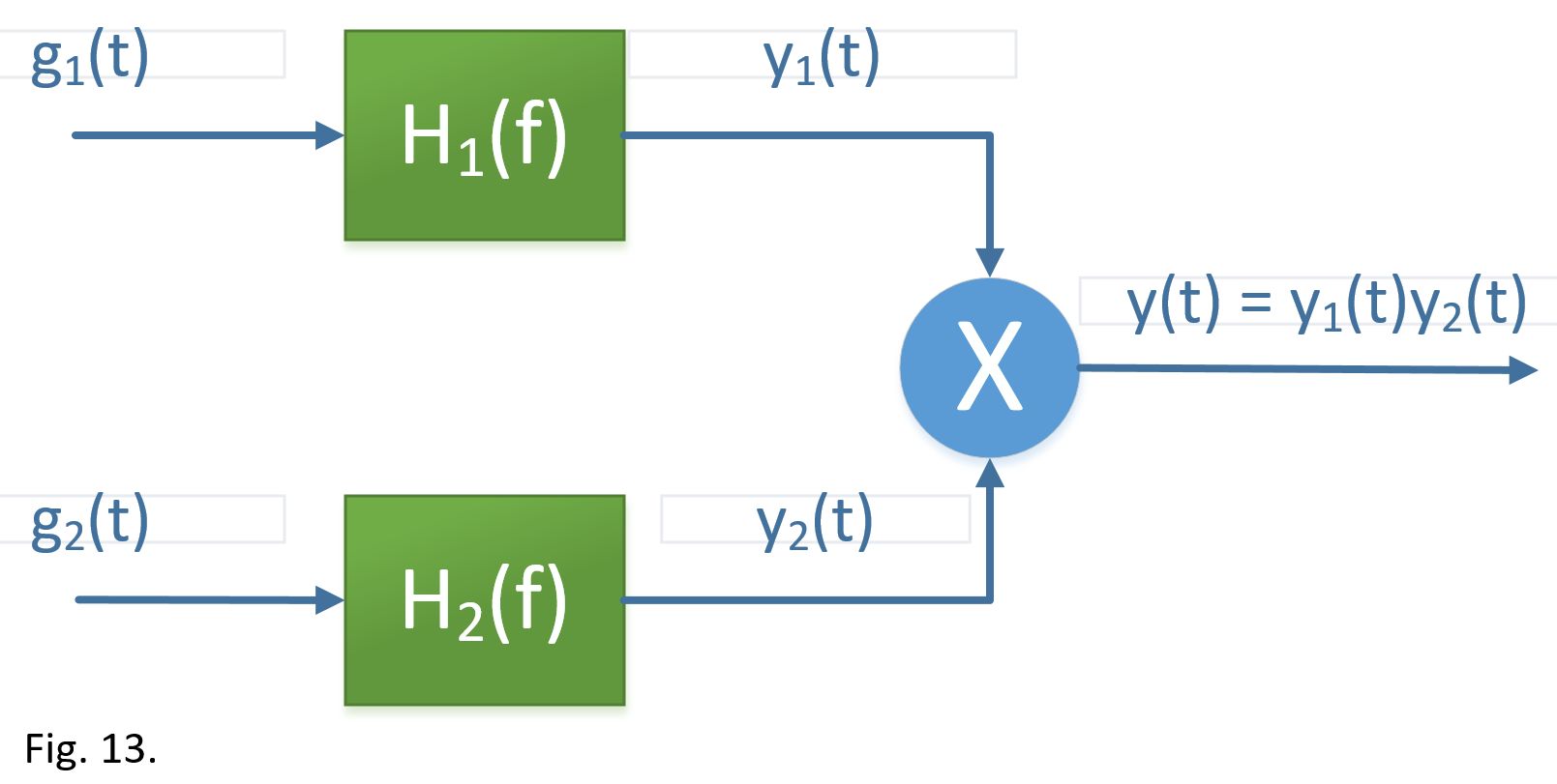
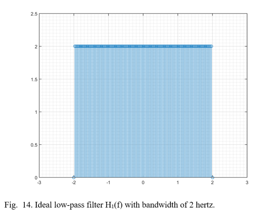
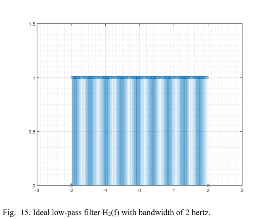
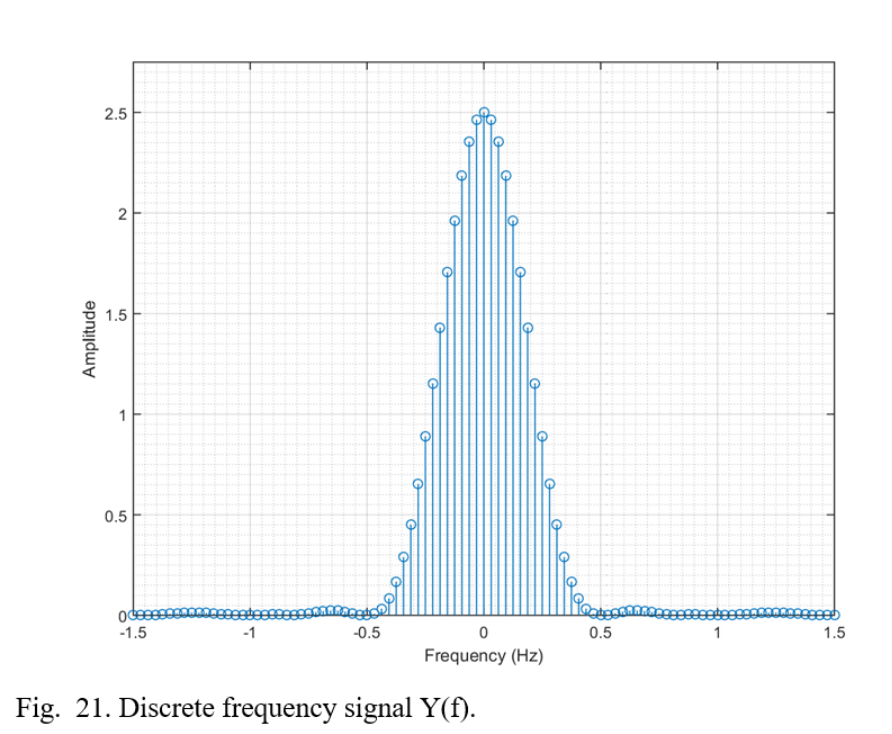
Now, let us consider the system shown in Fig. 13.
The blocks labeled H1(f) and H2(f) are ideal low pass filters with a bandwidth of 2 hertz.
The discrete frequency representation of the filters can be seen in the following figures
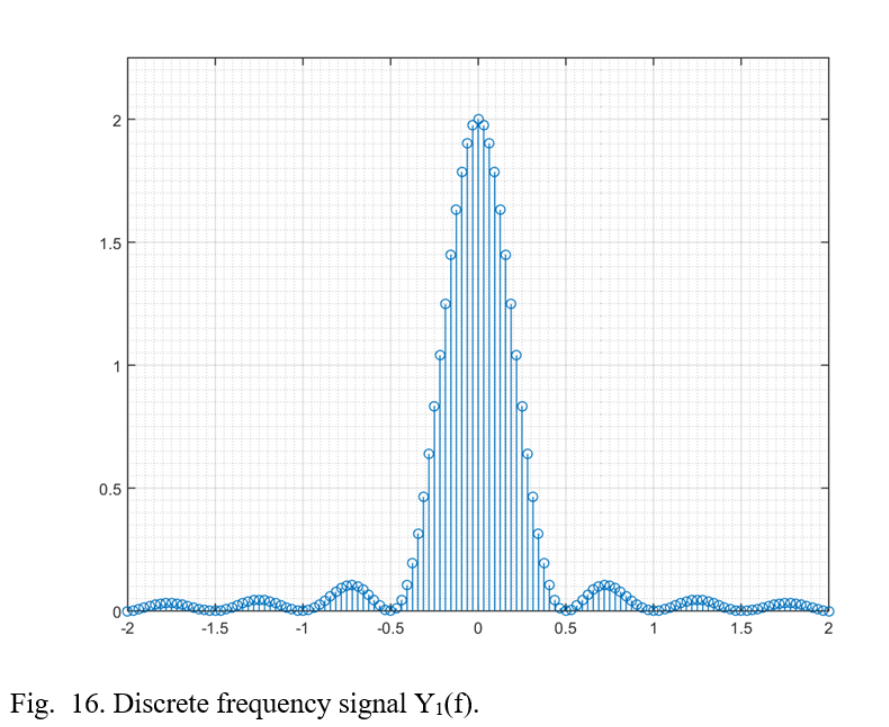
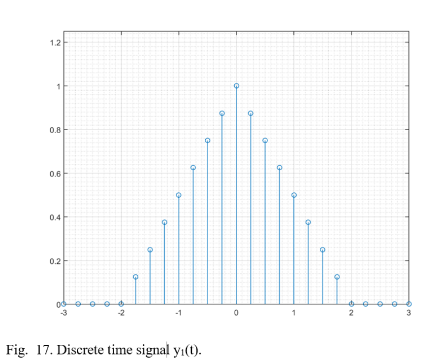
Passing the signal G1(f) through the ideal LPF H1(f) results in the following discrete waveform
Performing an inverse FFT on the signal Y1(f) = G1(f)H1(f) results in the following signal y1(t)
Reconstructed in this fashion, it can be seen that the signals g1(t) [Fig. 3] and y1(t) [Fig. 17] are remarkably similar even with all frequency components greater than/less than 2 hertz removed from y1(t).
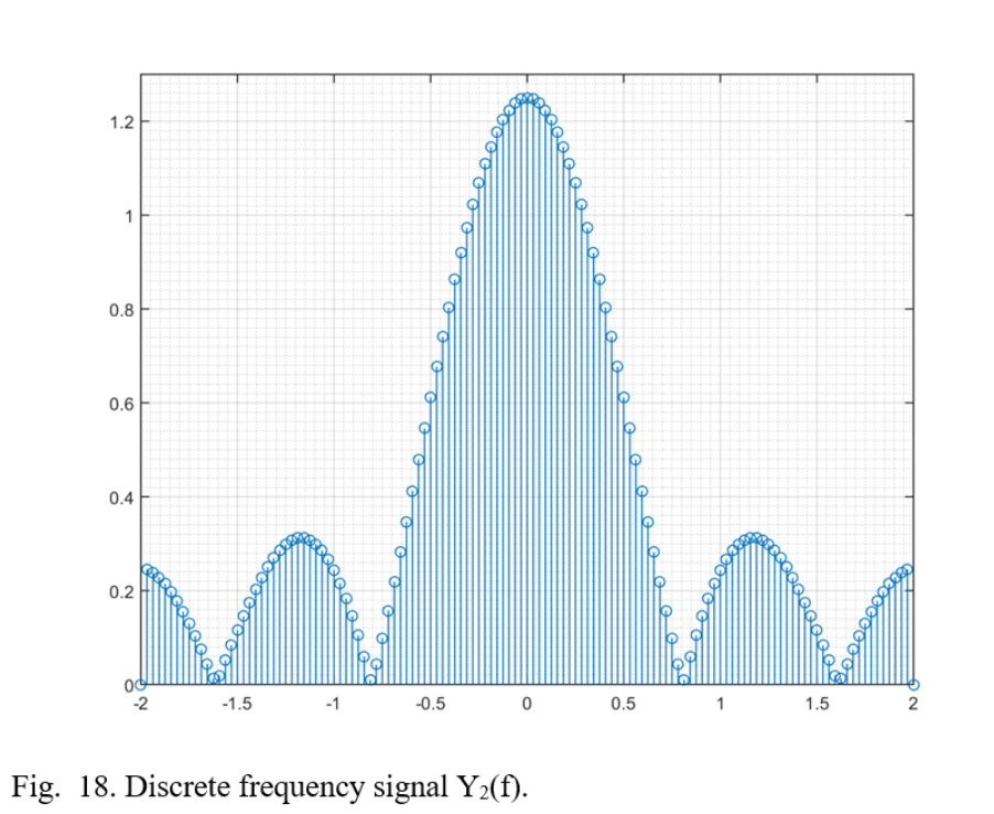
Passing the signal G2(f) through the ideal LPF H2(f) results in the following discrete waveform
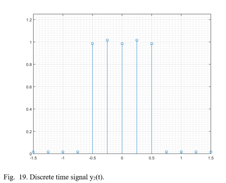
Performing an inverse FFT on the signal Y2(f) = G2(f)H2(f) results in the following signal y2(t)
Unlike the previous example with g1(t) and y1(t), it is evident that there are some imperfections resulting from the reconstruction of y2(t). This could be due to the fact that the ideal low-pass filter with a bandwidth of 2 hertz was not able to capture the signal in its entirety. Signals that exhibit abrupt changes in time, such as the changes that occur around the corners of the rectangular function, require higher frequency (energy) components. Filtering out these components will produce smoother and more oscillatory like behaviors in such areas.
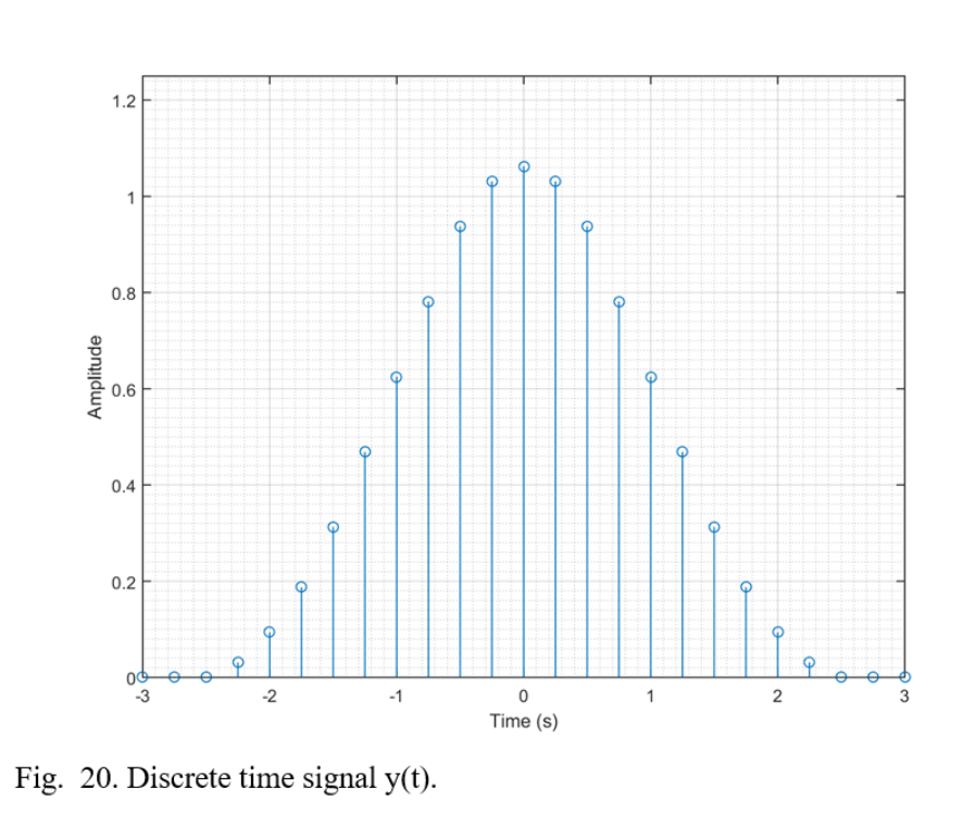
Mixing y1(t) with y2(t) results in the signal y(t). The following figures illustrate both time and frequency domains of the final signal
Conclusion
In order to effectively process continuous signals on a digital system, the signal bandwidth must be known. By applying the Nyquist-Shannon sampling theorem and Parseval’s theorem, the essential bandwidth of a signal can be defined and a sampling rate can be chosen. Choosing a sample rate that is too high will unnecessarily increase the demands on the processor and amount of memory required, while choosing a sample rate too low will result in loss of information and aliasing.
It should be noted to the reader that the FFT function contained within the MATLAB software requires special attention when attempting to properly scale in both time and frequency.
When performing an FFT, it is necessary to first perform an FFT Shift with the FFT of the desired signal inside its argument. For example
G1 = fftshift(fft(g1));
When attempting to plot a function in the frequency domain that resulted from a time domain function, such as the one above, the magnitude of the signal must be scaled down by a factor of the sampling frequency. For example
fs_g2 = 4; %sampling frequency for g2
normalize_g2 = fs_g2; %normalizing factor
G2_scaled = (G2)/normalize_g2; %divide G2 by normalizing factor
References
[1] “Communication in the presence of noise”, Proc. Institute of Radio Engineers, vol. 37, no. 1, pp. 10–21, Jan. 1949.
[2] Parseval des Chênes, Marc-Antoine “Mémoire sur les séries et sur l’intégration complète d’une équation aux différences partielles linéaire du second ordre, à coefficients constants” presented before the Académie des Sciences (Paris) on 5 April 1799.
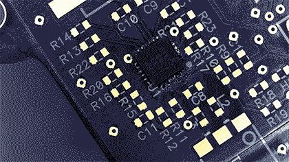
When soldering a package that has many pins, it is advantageous to use solder paste and hot air, as many pins can be soldered at the same time. While this method may create bridging or leave some connections unsoldered, applying flux and dragging an iron slowly across all of the pins is usually enough to fix any issues. As always, clean up the left over flux with 99% isopropyl alcohol or naphtha.
Soldering a 24 pin TQFN package with solder paste and hot air:
When you have pads that are entirely covered by the part package, or even mostly covered, your only choice is to reflow with hot air or an oven. The approach is similar to the previous example, however, you should take extra care to ensure your connections are aren’t shorted given that you cannot visually inspect them. You can ohm out the pins with a multimeter before applying power to be sure that you won’t damage your part.
For packages that don’t have a tremendous amount of pins, you may just want to use your iron and solder. In this demonstration I am soldering pin by pin. There are other techniques with an iron that involve pre-loading the tip with solder and steadily dragging across the pins. This method is fast and efficient, but requires special soldering iron tips such as this one: T15-CF4
Soldering SMD resistors, capacitors, and inductors can also be done with an iron or paste/hot air. When soldering with an iron, you want to apply solder to one pad and let it cool. Grab your part with tweezers and then liquefy the solder again with the iron as you use your other hand to slide the part over the pad. Once the solder cools again, remove the tweezers and your part should be held in place. You can now apply solder to the other side of the part to finish the connection.
Why automate tests?
Automating tests on your bench is beneficial for a number of reasons:
You can collect more data in less time.
Mitigate human error.
Real-time data processing.
Data can be organized and exported in predefined formats.
Free up time to work on another part of the project or take a break.
How can I automate my tests? First, you need instrumentation that is programmable. Your instrument is programmable if there is a communication port on it that allows for at least one way data transmission. There are a variety of software tools available to send and collect data from them, both free and paid.
In industry, it is common for companies to use National Instrument’s LabVIEW, Keysight’s VEE, or even Matlab for writing test automation programs. LabVIEW and VEE are both graphical programming languages specifically designed for automated testing, measurements, data analysis, and reporting. Matlab is most commonly found in academia, however, you will sometimes find Matlab in companies who have a lot of legacy code.
You don’t need expensive software to automate your own tests at home (or at work for that matter). Any programming language that can send and receive data through your USB or RS232 port will suffice, however, some are better than others.
Pythonis a powerful language that lends itself to this sort of task. There is a python library called ‘PyVisa’ which allows you to easily communicate with programmable instruments by use of the NI VISA drivers. Using the PyVisa library in conjunction with NumPy, SciPy, MatPlotLib, and OpenPyXl offers a very powerful tool for gathering and processing data obtained from programmable test equipment. If your instrument operates off of a non-ASCII text based protocol, such as Modbus, you can use the pySerial library to send and receive each byte, and even find yourself a CRC algorithm already written for you in python!
What is VISA? VISA stands for Virtual Instrument Software Architecture. It is a standard developed by National Instruments for configuring, programming, and troubleshooting instrumentation. It can interface by means of USB, Ethernet, Serial, GPIB, VXI, or PXI. The NI VISA drivers are free to download and use with your programmable instrument, even if you are not using NI LabVIEW.
Okay… I’ve heard enough. How about an example? Let’s say you have just designed an amplifier circuit and you want to characterize its amplitude response for a range of input frequencies.
Easy.
You can write a python script that utilizes the instruments’ SCPI commands to systematically characterize the amplifier’s gain for a given range of input frequencies.
SCPI stands for Standard Commands for Programmable Instruments. It is a standard by which instruments can communicate with a computer using ASCII text strings. Most instruments today use this standard and will come with a programming manual that tells you all of the SCPI commands that the instrument understands when it is put into ‘remote’ mode.
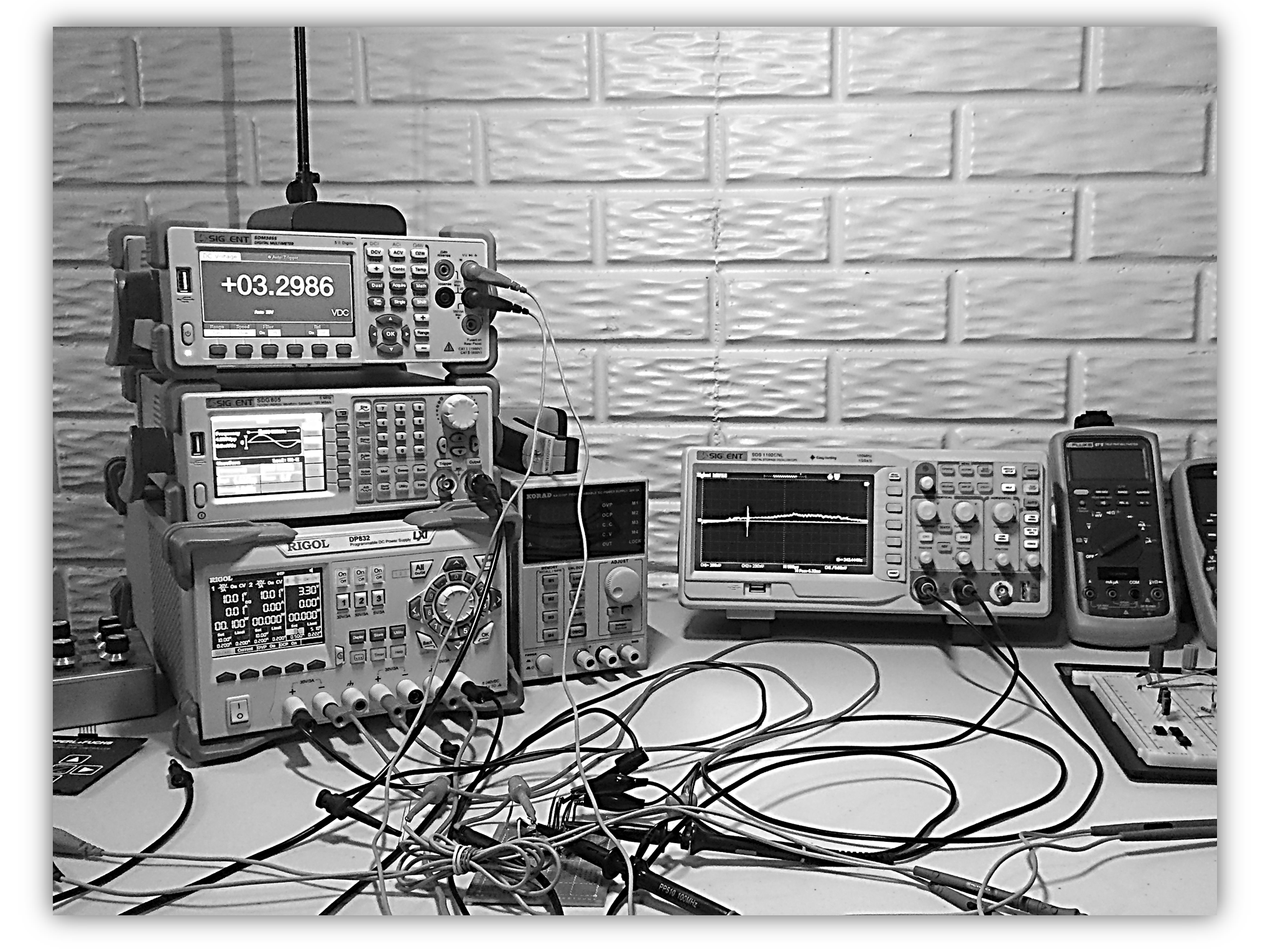
For this example, I will be using the following equipment:
Click on each of the instruments to see the python functions I have written for them. The function prototypes can be found here.
Note that if you happen to have the same instruments as me and would like to use my code, you may have to change the resource name for your instrument:
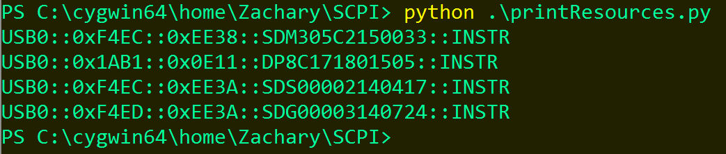
I have written a script that will output the resource names for all of your connected instruments. It can be found hereon my github page.
Here is an example of what the output might look like when you run the script:
For this test, I will need to be able to remotely carry out the following functionalities:
Set power supply voltage
Set power supply over current protection
Toggle power supply channels on/off
Set waveform generator amplitude and frequency
Toggle waveform generator channel on/off
Measure peak to peak voltages from both channels of the oscilloscope
Once all of these have been written in, I can call these functions sequentially in the test script just as if I were preforming the task by hand.
The test script for characterizing the gain of the amplifier can be found here.
To summarize what will happen in this test:
Over current protection is set and the amplifier is given power from two channels of the power supply.
The amplitude of the input signal is set to 4 mV and the frequency is set to 1 Hz.
A peak-to-peak voltage measurement is taken by the oscilloscope of both the input and output signals of the amplifier.
The frequency is increased by 100 Hz, and the input and output peak-to-peak voltage is measured again.
This process is repeated until the frequency of the input signal has reached 1 MHz.
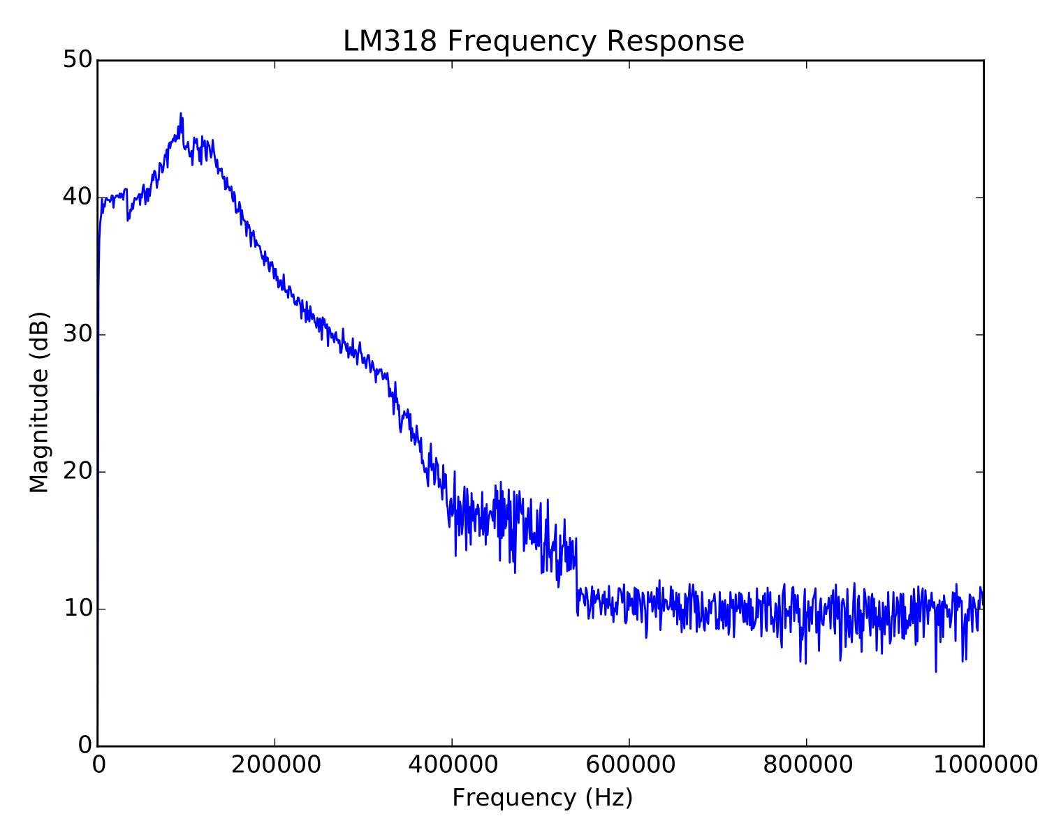
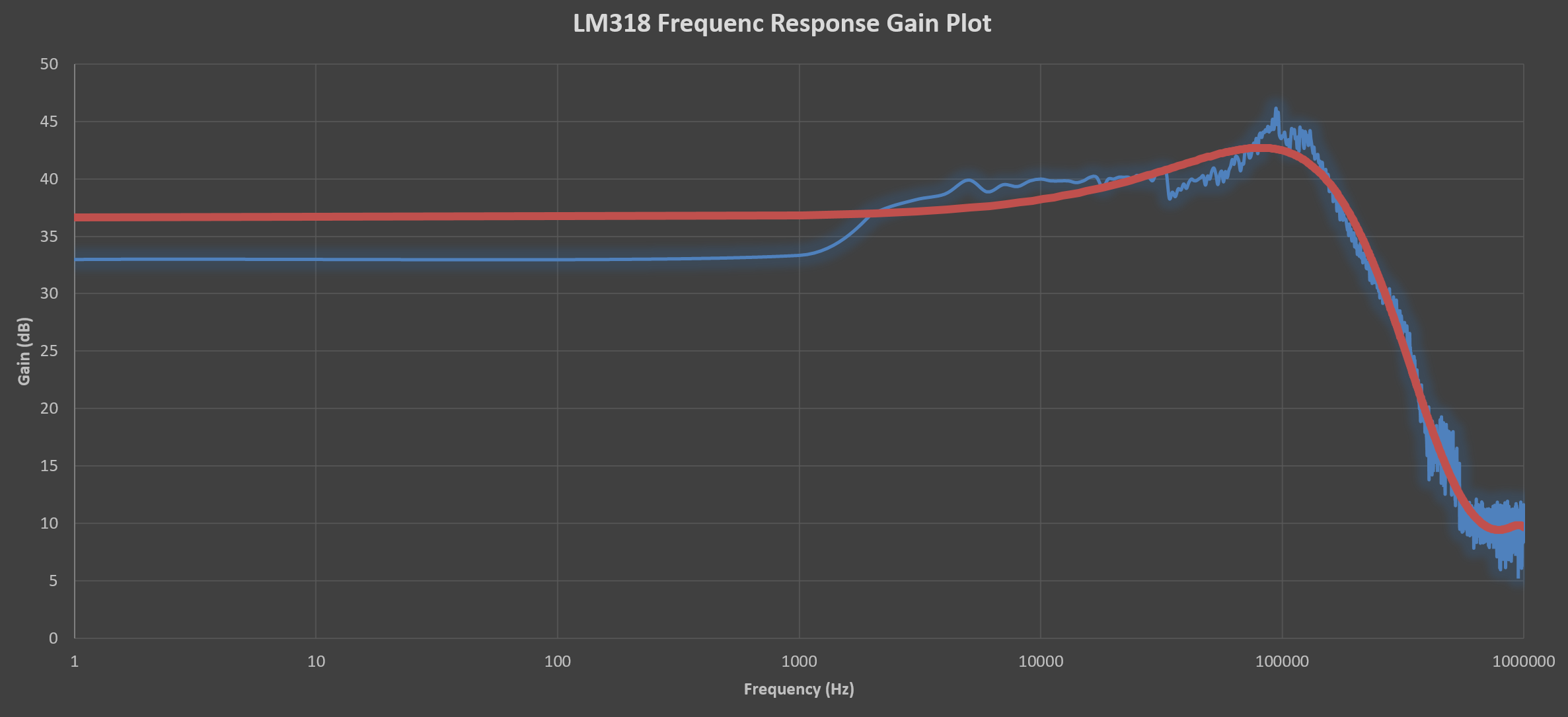
Once the test has been completed, the raw data is automatically exported into an Excel file in addition to generating a scaled plot with a title and axis labels and then saving this plot as a PDF file. The auto-generated plot is so that I can easily visualize the data to see if what I collected is meaningful.
Turn off the power supply and waveform generator’s outputs.
It should also be noted that calculations can be performed on the data as it is collected. In this example, I am calculating the gain in dB after each input and output peak-to-peak voltage reading is taken, and then storing the result in an array.
Here is what the auto-generated plot looks like:
I now have an idea of what my data looks like and every data point has been saved into an Excel spreadsheet. Now I can do what ever I want with the data — create more plots, add trend lines, etc…
Conclusion Test automation is a valuable skill to have in your tool belt. If you are a designer, chances are you are going to be spending a lot of time validating your design requirements. While the programming requires a significant amount of effort in the front end, you will surely save time in the long run and become a more capable designer and tester.


